2026.09.23 | Substack | Memory | HBM Hybrid Bonding Expert Call
原标题:[Expert Call Report] HBM Hybrid Bonding: From Technology to Volume Production
The Starting Question

HBM Density Peak: Why AI Value Is Moving From Memory to Connectivity
Damnang
Aug 20
If HBM stacks move to eight or even four layers, will that delay the adoption of hybrid bonding? This was one of the questions I wanted to explore in this expert call.
In this conversation, we discussed hybrid bonding technology from several angles, with a particular focus on HBM.
We covered when hybrid bonding is likely to be adopted in HBM, what is currently holding back the transition, what needs to change in terms of process equipment, how large the current technology gap is between Samsung and SK hynix in HBM, and why Besi has become one of the most closely watched hybrid bonding equipment suppliers.
The expert views 2026 to 2030 as a key transition period for HBM hybrid bonding and believes it will ultimately become an essential technology. We go through the technical details and practical challenges behind that transition in the report below.
Key Takeaways
- The number of layers alone does not determine the need for hybrid bonding.
The expert identified height and thermal performance as the main drivers for HBM today, while describing a separate adoption condition for products that require finer pitch.
- Maturity in bonding a single layer is not the same as readiness to produce multilayer stacks.
Beyond the economics of the existing process, the expert highlighted the challenge of maintaining quality across a combination of process steps.
- Running one tool well and bringing multiple tools into consistent operation are different tasks.
In addition to managing contamination during repeated operation, engineers have to identify and resolve differences between the tools they install.
- Besi’s strength lies in improvements accumulated through actual production experience.
The expert distinguished that experience in logic bonding from the final equipment selection for multilayer HBM.
- Current challenges should be considered alongside the longer term transition.
The expert personally sees 2026 to 2030 as an important transition period and described improvements to existing TCB processes and preparation for hybrid bonding as parallel efforts.
Editorial Note
The questions and answers have been organized by topic from the original transcript. “Damnang’s Commentary” presents the editor’s interpretation of the interview. The expert’s explanations and outlook reflect his personal views at the time of the conversation, not the company’s official position. Generative AI assisted with language editing and organization.
Damnang Research is a reader-supported publication. To receive new posts and support my work, consider becoming a free or paid subscriber.
 Subscribed
Damnang
Mar 29
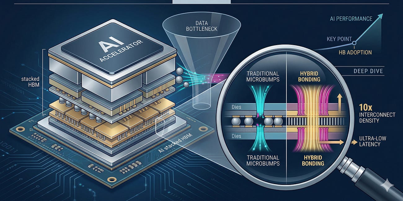
If you had to name the single hottest keyword in the semiconductor industry right now, I’d say hybrid bonding without hesitation.
Do Fewer Layers Reduce the Need for Hybrid Bonding?
The Basics | Hybrid Bonding and TCB
The expert described hybrid bonding as a process that bonds both copper and dielectric materials. CMP makes the surfaces flat, followed by plasma treatment and cleaning to prepare them. The dielectric surfaces are bonded first, and subsequent heat treatment forms the copper bonds.
By comparison, thermocompression bonding, or TCB, uses heat and pressure to bond solder interconnects. Pitch is the spacing between adjacent interconnects.
Damnang: What are the main reasons for considering hybrid bonding in HBM?
Expert: Hybrid bonding is well suited to reducing interconnect pitch. For HBM today, however, I see height and thermal performance as the biggest factors. I do not think an increase in the number of I/Os necessarily means that hybrid bonding must be adopted.
HBM has to fit multiple dies within a specified height. If that height limit is relaxed, there may be more room to continue using the existing process. Conversely, if customers want more layers, the need for a technology that reduces height becomes greater.
Thermal performance is another important reason. The literature describes an improvement of about 20% in thermal performance with hybrid bonding. There is also room for further improvement, for example by changing the dielectric materials.
Editor’s note: The approximate 20% thermal improvement is a figure the expert cited from the literature. The specific metric and comparison conditions should be interpreted in the context of the relevant publication.
Damnang: Do efforts to improve thermal performance also involve changes to the bonding interface or materials?
Expert: The layers and interfaces within a chip contain various dielectric materials, and those materials can impede heat removal. That is why there are efforts to replace materials at the bonding interface or between layers with ones that conduct heat more effectively. Aluminum nitride and boron nitride are examples.
However, an improvement in thermal performance can come with problems in other electrical properties or leakage. Changing a material also means establishing the process conditions for it again. Even changing a single material is not straightforward.
Damnang: If the stack is reduced to eight or four layers, might hybrid bonding no longer be necessary?
Expert: That could be the case from a height perspective, but the number of layers alone is not enough to decide.
I do not study AI workloads directly. I have heard, however, that capacity and bandwidth requirements differ by application. For example, we can imagine a product that places greater emphasis on bandwidth than on capacity.
If such a product requires an interconnect pitch finer than the existing process can support, hybrid bonding becomes necessary even with fewer layers. In that case, pitch rather than height drives the change in bonding method.
Damnang: How fine does the pitch have to become before you would consider moving away from the existing method?
Expert: I see roughly 10 micrometers as one threshold. Different people may have different views, but I would put the range at about 5 to 10 micrometers.
Existing TCB processes use solder to form the interconnects, which makes very fine pitch difficult to achieve. If a product requires a pitch beyond what that method can support, there comes a point when it has to move to hybrid bonding.
For HBM today, however, I do not see that degree of pitch scaling as the main requirement. That is why I identified height and thermal performance as the more important factors earlier.
Damnang: So hybrid bonding can increase bandwidth because it allows more connections between dies?
Expert: Correct. Bonding at a finer pitch allows more interconnects between dies within the same area. The ability to make those connections much denser is a major difference from the existing method.
Damnang’s Commentary
Lower stack counts can reduce the height constraint, but that does not necessarily mean thermal requirements or interconnect density move in the same direction. The key takeaway from this discussion is that stack height, thermals, and pitch can each influence the choice of bonding technology for different reasons.
I have also recently heard industry chatter that some customers are raising concerns about HBM heat dissipation, particularly at the rack and system level. This is why I think the question should not stop at “How many layers does the product need?” We also need to ask what thermal characteristics and interconnect pitch the product requires.
Even with a lower stack count, thermal requirements alone could still justify the use of hybrid bonding. Alternatively, the need for higher bandwidth could require much finer interconnect pitch. Ultimately, I believe these evolving customer requirements could become the trigger that drives the transition toward hybrid bonding.
Why Is the Transition to HBM Hybrid Bonding So Difficult?
Damnang: If hybrid bonding offers advantages in height and thermal performance, why do manufacturers want to keep using the existing method for as long as possible?
Expert: Because they have already invested heavily in the existing process. They have installed equipment, resolved problems, and accumulated expertise in making products with those tools. From a manufacturer’s perspective, it makes sense to get as much use as possible out of that foundation.
If improving thermal performance requires major changes across the process, the cost burden is substantial. As long as the existing method can meet customer specifications, manufacturers want to keep using it and switch only when necessary. In some respects, hybrid bonding feels a little ahead of its time for HBM.
Damnang: So changing the established process carries a substantial cost. How about the technology itself? Would you say hybrid bonding is already close to fully developed?
Expert: If we are talking about bonding a single layer, I think the technology is quite mature. It is well documented in the literature, and it is already used in volume production in applications such as image sensors.
The situation changes when you start stacking multiple layers, as in HBM.
Having a mature technology for bonding one layer is different from being able to maintain quality consistently while stacking eight, 12, or 16 layers.
In that sense, my personal view is that reliable volume production of multilayer stacks is still some way off.
Damnang: So maintaining quality while stacking multiple layers and preparing that process for volume production are still difficult?
Expert: Yes. Even during development, there are so many process steps that it is difficult to identify immediately where a problem began. You also have to determine which conditions in which process need to change to resolve it.
Multiple processes affect one another, producing a variety of problems. It is still not easy to pinpoint exactly what needs to change to improve the result.
Looking at the overall picture, development is clearly progressing. But from the perspective of someone working through the process conditions one by one, there is still a great deal to resolve.
Process Development Continues After the Equipment Arrives
Damnang: What has to change most on the equipment side to move to hybrid bonding?
Expert: The most direct change is to the bonding equipment. For processes such as CMP, dicing, and CVD, the task is largely to optimize existing equipment and technology for HBM. But it is difficult to convert an existing TCB tool directly into a hybrid bonding tool.
Put simply, a bonder has to pick up a thin die and place it accurately in the intended position. Think, for example, of a die 30 to 50 micrometers thick and approximately 10 to 15 millimeters in size.
First, the precision requirements are different. As an illustration, to bond at a pitch of 1 micrometer, you can think of the tool as needing precision of about 200 nanometers. The question is whether the installed equipment was designed to meet that requirement.
The cleanliness requirements are different as well. You have to manage not only the cleanliness of the bonding surfaces, but also particles generated inside the equipment.
Editor’s note: The die dimensions, pitch, and tool precision figures are examples the expert used to explain the bonder’s task and the level of performance required.
Damnang: What does “it has to be clean” actually mean in day to day work?
Expert: A great deal of cleaning. A surface can look clean to the eye, but a UV lamp can reveal fine dust that you thought was not there. You have to keep finding and managing that contamination.
The process may initially deliver good results, but particles can be generated as more products are processed. Then, at some point, the process results deteriorate. When you investigate, you find that the tool has become contaminated.
You clean the equipment and check it again. If that is not enough, you clean it again. That process alone involves a substantial amount of work.
So this is not just about cleaning. The internal airflow also needs to be designed so that particles can leave the tool effectively. Existing equipment may not adequately incorporate that kind of design.
Damnang: Does the equipment configuration also change for hybrid bonding compared with existing TCB processes?
Expert: For TCB, we often used standalone tools with separate equipment for different process steps. A wafer might undergo plasma treatment in one tool, then move to another tool for bonding.
For hybrid bonding, there is a great deal of discussion about cluster systems that carry out plasma treatment, cleaning, and bonding sequentially within one system. They may also include UV treatment to reduce tape adhesion so that thin dies can be picked up, as well as metrology where needed.

The Kinex integrated hybrid bonding system, shown in an official product rendering published by Applied Materials. It illustrates the appearance of a cluster system and is not a photograph of equipment installed at a particular customer.
Damnang: What are the advantages of carrying out multiple processes within one system?
Expert: First, it narrows the set of tools you need to investigate when a problem occurs. When a wafer moves between several tools, it can be difficult to identify which one caused the issue. If the process took place within one system, you can start by investigating that system.
There is also a time limit between plasma treatment or cleaning and bonding. We call this queue time. Moving directly to the next step within one system helps manage that interval. The time constraint is not always extremely tight, though, and equipment suppliers tend to emphasize this benefit.
From a development perspective, not having to repeatedly load, unload, and move material between tools is a major advantage. With separate tools, you load the plasma tool, unload it, and then move the material to another tool and load it again.
For example, work that takes one or two hours that way might run in 10 to 20 minutes when the steps proceed sequentially within one system. For someone repeating those tasks, that is a very practical difference.
Editor’s note: These times are examples of development work described by the expert, not an official comparison of production equipment throughput.
Damnang: Even with those advantages, it sounds as though a lot of work remains between bringing in equipment and operating it reliably. Did the existing TCB tools go through that process as well?
Expert: Yes. I have seen existing TCB tools being installed, adjusted, and put into volume production. The work did not end when the equipment arrived.
Even units of the same equipment can differ once they arrive. From the outside, you might ask why tools built the same way would differ, but in practice they do. The cause of those differences is not always immediately clear, either. Finding the cause and bringing the tools into alignment takes more time.
The TCB tools in operation today went through that process. Even after installation and initial adjustment, people have continued identifying causes and making improvements whenever problems arise.
Damnang: So after all that work to get the existing TCB tools running properly, introducing new equipment for hybrid bonding requires another substantial effort and investment.
Expert: Exactly. The cost is significant, but finding space for the equipment is also a major issue. You first have to decide where the new tools will go and whether other equipment needs to move to make room.
Then you need to coordinate equipment delivery, installation, and setup. Investing too early can also be a problem. If the equipment is ready but is not yet generating revenue, people may ask why the investment was made so soon.
From the outside, people can describe it simply as a transition to hybrid bonding. On the factory floor, however, you have to work through where to put the tools, when to bring them in, and how to adjust and operate them, one issue at a time.
Damnang’s Commentary
This explanation highlights two equipment challenges. One is maintaining cleanliness and process quality during repeated operation of a single tool. The other is identifying and resolving differences between multiple tools after installation. The latter came from the expert’s experience of expanding and stabilizing existing TCB operations.
Achieving good results on one tool is not the same stage of development as bringing multiple tools into reliable production. Assessing production readiness therefore requires looking beyond bonding precision to repeated operation, differences between tools, installation, and setup. The “production experience” emphasized by the expert in the next section can be understood in this context.
What Does Besi’s Production Experience Mean?
Damnang: Many companies make similar bonders. Why does Besi receive particular attention?
Expert: The goals for a bonder are broadly similar. It needs good precision, control of particles and voids, and sufficient processing speed. You can think of a void as air trapped at the bonding interface.
The published equipment specifications may not look dramatically different. But having operated in an actual production line means the tool has gone through many rounds of problem solving and improvement.
What I most want to emphasize about Besi is its production experience. I place importance on its experience in logic bonding production with TSMC.
Building a tool and refining it so that it keeps running on a customer’s production line are very different things.
Damnang: How do equipment suppliers and semiconductor manufacturers work together to reach that point?
Expert: They may work through a joint development project, or JDP.
For example, a supplier can install a tool at the manufacturer under an agreement that the manufacturer will buy it if it meets specified process goals for a particular product by a certain date. If those goals are not met, the development period may be extended or the equipment returned.
Throughout that process, the tool is continually improved to suit the actual product and process. It can be very different after development from when it first arrived.
Equipment is evaluated in different ways, too. There may be a simple demonstration, installation for joint development, or a purchase. These should not all be treated as the same stage.
Damnang: Does production experience in logic mean the equipment can be applied directly to HBM?
Expert: It does not transfer unchanged. Bonding a single layer for logic is different from stacking multiple layers for HBM. Moving to multilayer stacking brings another set of problems. Even with that existing experience, there are still issues to resolve specifically for HBM.
Damnang: Then can we say Samsung and SK hynix have already settled on Besi for their HBM hybrid bonding equipment?
Expert: We can say that Samsung and SK hynix use Besi equipment, and that Besi has production experience with TSMC.
But both companies are also exploring other equipment suppliers. Using or evaluating a tool today is different from deciding what equipment will be used in future production. The final supplier lineup for volume production remains undecided.
Damnang: As production scales up, pricing could also change the outcome.
Expert: Yes. Applied Materials provides modules such as robotics, plasma treatment, cleaning, and metrology, with Besi’s bonder integrated into that system. The price of that integrated equipment is also an important consideration.
When the available alternatives are limited, a manufacturer may choose it even at a high price. But we do not know how that will play out in volume production. Price competition matters as well.
Damnang’s Commentary
The expert’s assessment of Besi focused more on its development history than on a simple comparison of specifications. He saw strength in the experience of encountering problems in an actual production environment and improving the equipment. The earlier discussion of contamination and differences between tools helps explain why that experience matters.
However, the product through which that experience was gained should be distinguished from the new application. Existing production experience in logic bonding can be an advantage in HBM development, but it does not automatically satisfy the requirements of multilayer stacking or the conditions for purchase.
When reading equipment news, the statement that a tool “has been installed at a customer” should be followed by a closer look at the stage involved. The questions below are based on the evaluation and adoption arrangements discussed in the interview. They do not imply that every agreement follows this sequence.

Customer Specifications and Samsung’s Integrated Capabilities
After examining equipment requirements and adoption conditions, the conversation turned to product specifications that vary by customer. Different combinations of customer requirements call for different choices of processes and equipment. We discussed Samsung’s integrated capabilities from that perspective.
Damnang: So HBM may not necessarily evolve toward more and more layers. The direction could depend on what customers need.
Expert: As a supplier, you ultimately have to prepare the product the customer wants. That requirement might concern the number of layers, pitch, thermal performance, or chip size.
When those requirements become specifications, we have to select the combination of processes and equipment that can meet them. But the combination customers want keeps changing. In that sense, I feel we are entering an era of customization.
Damnang: Samsung has memory, foundry, packaging, and design capabilities within the same company. Can that structure be an advantage?
Expert: I think there are definite advantages. Among ourselves, we sometimes compare Samsung to Gimbap Cheonguk, a Korean diner with a broad menu. It offers many things, which does not mean each one is the best. Still, there is value in being able to choose different things together.
Different customers want different things. Some may want only memory. Others may want their base die made at another foundry. And some may want several elements supplied together.
Having a range of technologies ready allows you to respond to those combinations. Offering individual technologies separately and offering the combination a customer wants are different forms of value.
Damnang: Does that integrated structure also help during development?
Expert: I do not work directly in design, but I have heard that getting logic, memory, and other elements to work together requires a great deal of communication. It involves repeated cycles of finding problems, identifying their causes, and making corrections.
In that process, having teams close to one another and able to work together is an advantage. It can be different from coordinating the same work across separate companies or countries.
Samsung continues to prepare a range of technologies. How that potential translates into results is a separate question, but I think having a broad set of options has value in itself.
Damnang’s Commentary
Samsung’s strategy is essentially a turnkey approach. It may not have the number one technology in every individual component, but for products like HBM, where multiple technologies need to be tightly integrated, I think this turnkey model can create a clear competitive advantage.
Consider a simple example. Suppose Samsung uses its own 2 nm process for the HBM5 base die. What would SK hynix need to do to match that capability? It would have to secure the logic process externally, coordinate development across different companies, and align design, process, and packaging requirements across organizational boundaries.
The key point is that Samsung can reduce much of that integration burden internally. From a technology perspective, simply being able to remove some of these coordination challenges can itself be a meaningful advantage.
Today’s Production Challenges and the Longer Term Transition
Damnang: Finally, will HBM eventually move to hybrid bonding? What will determine the timing?
Expert: I believe it will definitely happen eventually. The timing, however, depends on what customers want. A supplier having a good technology ready does not, by itself, make adoption happen.
Personally, I see 2026 to 2030 as an important transition period. I expect that by around 2030, we may look back and say, “Quite a lot of progress has been made.” This is my personal outlook rather than a firm schedule, but I think there will be a great deal of change during that period.
Up close, there are many problems to resolve today. But with time, the process may have moved a long way forward. In my view, semiconductor process development progresses by committing people, time, and money, then resolving the problems that arise one by one.
Damnang: So improving the existing TCB process and preparing for hybrid bonding are happening in parallel.
Expert: That’s right. Samsung has also become much better at TCB and is already executing it well. At the same time, the company has been investing in hybrid bonding for years, and multiple teams are still working to bring HBM hybrid bonding into production.
Through that process, Samsung has accumulated a significant amount of practical know how. This is not something a competitor can simply replicate by hearing how the process works. It has to be built through repeated development, troubleshooting, and manufacturing experience.
Based on what I have been hearing from the industry, the gap in hybrid bonding capability between Samsung and some of its competitors may already be quite significant.
Damnang’s Commentary
In the follow up expert call with an SK hynix advanced memory process development engineer, I was able to further confirm that Samsung currently appears to hold a much stronger position in hybrid bonding.
Samsung has reportedly already delivered hybrid bonded HBM4 and HBM4E samples to customers, while SK hynix is not yet believed to have reached the sample stage.
If hybrid bonding is ultimately the direction HBM must take from a technology standpoint, this gap could become increasingly important. One of the key things to watch will be how the current gap in hybrid bonding capability translates into actual competitive outcomes in HBM5 and 3D stacked DRAM.