2026.09.24 | Substack | Memory | SKHY In-House 2.5D Packaging
原标题:SK hynix's In-House 2.5D: Validation Comes Before Commercialization
At the afternoon roundtable of SK hynix’s Global Forum, held in the US on September 18, two questions from the audience were really about the same thing. One asked whether a bigger role for Indiana might shake the company’s relationships with its foundry partners and customers. The other was blunter. At last year’s forum the company had said it wouldn’t do logic because the TSMC ecosystem works well, so had things gone bad with TSMC, and was that why it was turning to in-house work?
Both answers went the same way. The point was that Samsung and Intel overlap with TSMC in their core business while SK hynix doesn’t, and that this is what makes it a good partner. The speaker said the company won’t go where it would overlap with TSMC, and has no plan to become a foundry just because its base dies are doing well. On the Indiana question, the speaker answered that the company doesn’t have the capability to do it right now, that it’s preparing step by step, and that you need the technology before you can even negotiate.
Those questions came up because, early in the roundtable, the speaker had said the company has been preparing a CoWoS-L class 2.5D package for two years. Last week, in [[Investment Map] 22 Listed Companies in the Hybrid Bonding Value Chain, I went through twenty-two companies in the hybrid bonding value chain. If hybrid bonding is about stacking chips upward,
- 5D is about spreading them out sideways. Let me give you the conclusion first. For now, the line’s purpose is to find
out firsthand under what conditions the company’s HBM fails inside customers’ packages, and the place to do that work is the R&D testbed in Indiana. That’s the answer I heard. Commercialization comes after that.

Contents
- What I Heard and What I Checked
- Where Part 1 Left Off
- What Has Been Built So Far
- Why Build It: Two Purposes
- The Weight of Yield, and Shift-Left
- The Work That Overlaps with Indiana
- Closing
- References
1. What I Heard and What I Checked
The event was an invitation-only session that doubled as recruiting, so I didn’t get the slides. That’s why every number and fact in this piece that carries a source number was checked against public material, and anything I only heard in the room is flagged as such. A good part of the talk overlaps with the slides an executive from the same company presented publicly at Hot Chips 2026 on August 23, so the broad outline can be checked against that public presentation [1].
The audience questions ended up focused on the TSMC relationship, but there’s something to look at before that: how far the in-house 2.5D has actually come, and why it’s being built. The idea that the relationship had gone bad was the questioner’s guess. The company never said so.
2. Where Part 1 Left Off
In Part 1, SK hynix’s Four Packaging Paths: Where Is the Fight After HBM?, I laid out four paths in advanced packaging, filed silicon bridges and 2.5D under Path 4, drew the map and left the rest for later. In August 2024 the company’s vice president in charge of packaging development was reported to have said in a lecture that the silicon interposer underneath 2.5D was close to a “chicken rib,” something of little use yet hard to throw away [2]. In December 2025 came a report that the company was pushing to build its first 2.5D production line in the US, and the company’s response was that nothing specific had been decided [3]. In May this year a Korean outlet reported that it was pursuing 2.5D packaging cooperation using Intel’s EMIB (Intel’s approach of burying a small silicon bridge in the package substrate to connect chips) [4], and the word 2.5D doesn’t appear even once in the official groundbreaking release of August 28 [5]. That release introduced the Indiana fab as an HBM production line plus an advanced packaging R&D testbed.
But at this roundtable, what came out was that the company has been preparing its in-house 2.5D for two years and that the Indiana fab will take the technology first. Going by public material alone, this is a company that called the interposer a chicken rib, said nothing had been decided about a US 2.5D line, and left 2.5D out of its groundbreaking release. Meanwhile, behind the scenes, it had been building a test vehicle, and this time the specs came out in some detail.
This Substack is reader-supported. To receive new posts and support my work, consider becoming a free or paid subscriber.
 Subscribed
3. What Has Been Built So Far
What the speaker compared the in-house 2.5D against was TSMC’s CoWoS-L. Starting with the name, CoWoS is what TSMC calls its 2.5D package. A logic chip such as a GPU and the HBM sit side by side on a thin intermediate board called an interposer, which wires them to each other, and that whole assembly then sits on a package substrate. The letter at the end tells you what the interposer is made of.
In CoWoS-S the entire interposer is one piece of silicon. It has the finest wiring of the three, but there’s a limit to how large you can make it, and the ceiling TSMC gives is about 3.3 times the reticle (the largest area a lithography tool can print in one shot). CoWoS-R uses a redistribution layer (RDL) made of polymer and copper wiring as the interposer instead of silicon. It’s easier to make large, but the wiring is coarser than silicon’s. CoWoS-L is the compromise, an RDL interposer with small silicon bridges (TSMC calls them LSI) embedded only where chips need a dense connection to each other [6].
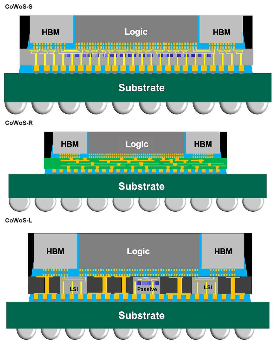
CoWoS-S, CoWoS-R and CoWoS-L structure diagrams from TSMC’s 3DFabric CoWoS page. Source: TSMC, retrieved September 23, 2026
The speaker said they can do CoWoS-S and CoWoS-R as well, but CoWoS-L volume is what’s growing in the market right now, so that’s the one they aimed at. They needed a way to test internally how far their HBM holds up inside a large package, and that’s why they built their own test vehicle.
Here are the specs of the first test vehicle. It’s 3.3 times the reticle, about 2,500mm² in area. It carries two chips that mimic an SoC and eight HBM sites, and the eight sites hold daisy-chain dummy chips rather than real HBM, chips that only check whether current flows properly through the wiring. Package reliability passed without major problems, and they’re now raising its maturity while making it bigger.
My take was that they’re further along than I expected. When I heard it was for validation I pictured something scaled down, but it’s almost the same size as the first CoWoS-L test vehicle TSMC demonstrated.
That size makes more sense next to TSMC’s public roadmap. The first CoWoS-L test vehicle TSMC demonstrated at ECTC 2023 (the IEEE Electronic Components and Technology Conference) was 3 times the reticle, about 2,500mm², with eight HBM sites [7]. The speaker’s 3.3 times and 2,500mm² don’t quite match each other, because TSMC puts 3.3 times, the CoWoS-S ceiling, at about 2,700mm² [6]. One of the two may have been a rounded figure. Whichever number you go with, what SK hynix is building on its own line now is about the size of TSMC’s first demo. The first CoWoS-L to go into volume production, in 2024, was a little bigger at 3.5 times the reticle [6], and what’s in volume today has reached 5.5 times with up to twelve HBM sites [8]. At TSMC’s OIP forum in late 2024 there was a plan to qualify a 9 times (about 7,700mm²) Super Carrier in 2027 [9], and later symposium roadmaps put 9.5 times in the same 2027 slot [8]. A roadmap is also public for 14 times with twenty HBM stacks in 2028, and more than 14 times with twenty-four HBM sites in 2029 [10]. So SK hynix is near the starting line, and TSMC’s volume lines are making much larger packages. The two lines are built for different purposes, though. On the SK hynix side it’s a daisy chain for validating its own HBM, and on the TSMC side it’s customers’ production parts. Similar size doesn’t mean similar maturity, so I won’t rank them on the same scale.
On the bridge side, the deep trench capacitor came up (DTC, a capacitor made by etching narrow, deep trenches into silicon; embedded in the bridge, it absorbs sudden changes in current and keeps the power supply stable). They’re developing it together with the company’s research institute. The first generation is around 1μF, and internally they’re validating levels above 2μF. If you want to build a large-area CoWoS-L class package, I think power stabilization parts are a must. TSMC, too, embeds eDTC (embedded DTC) under the SoC and inside the LSI bridges in CoWoS-L to secure power stability [6][7]. Intel takes a different approach, drilling TSVs (through-silicon vias, vertical connections that pass through the silicon) into the bridge to open a path for power (section 6).
Putting what I heard together, an in-house CoWoS-L class test vehicle about the size of TSMC’s first demo has passed reliability, the DTC for the bridge is being developed with the company’s research institute, and this line goes to Indiana first. The speaker also said they’re talking to customers with it and are at the stage of trying tests with a few customers who showed interest. None of this is in the official releases. It came up only at the roundtable.
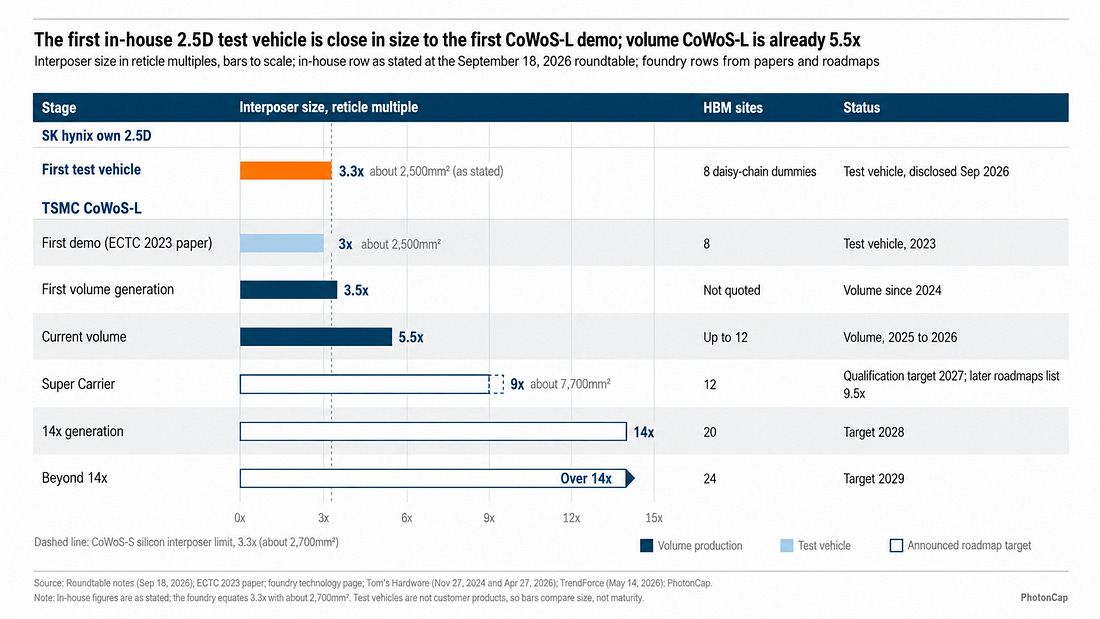
SK hynix’s first 2.5D test vehicle is about the size of TSMC’s first CoWoS-L demo, while TSMC already produces 5.5x. Reticle-multiple bar ladder
4. Why Build It: Two Purposes
The first is that it’s hard for the company to know how well its HBM holds up inside a customer’s large-area package. As the speaker explained, HBM has become the most vulnerable part in the package now that it sits right next to the GPU, yet the information on how that package is built and how heat flows through it sits with the foundry and the customer. So only by running a large-area 2.5D package on its own line can the company predict where and how its HBM will run into trouble. It’s closer to regression testing, working back through quality and design.
The second is building capability as a candidate for a new business model. This is where the supply shortage comes in. The way it was put in the room: “When we try to get R&D capacity allocated with certain companies in Taiwan, it’s all allocated to very big customers, so it isn’t easy for startups or second-tier players to get work done.” That matches the direction of the public data. According to a Taiwan Economic Daily report relayed by TrendForce in June 2026, institutional investors think that even if TSMC’s monthly CoWoS capacity rises to 120,000-140,000 wafers in 2026, the supply-demand gap will only narrow from about 20% now to about 10% by the end of 2026 [11]. TrendForce’s own view is that the 2.5D packaging shortage eases around 2027. A September report said capacity would double, from around 130,000 wafers a month at the end of 2026 to 260,000 by the end of 2028 [12], but the feeling in the room that even within that capacity, second-tier players and ASIC startups have a hard time getting a slot on Taiwanese lines doesn’t contradict the public numbers.
The speaker also added something, framed as a personal opinion. These days the HBM inside a SiP (system in package, several chips assembled into one package) costs more than the GPU die, and HBM is also the most vulnerable part, yet SiP design is still based on the GPU and the HBM has to fit into it. So why not fit the SiP to the HBM instead? The gist went like this. If you hand production HBM tuned for the first customer to second- and third-tier customers as is, you get requests like “it doesn’t fit, please change it,” and that takes time, so you might as well use that time to build a package around the HBM on your own line first.
Here’s what I think. Whoever holds the key gets to lay out the board, and that means the GPU customer, so I see the odds of this happening as low. Still, the fact that memory-centric package design is being discussed on the ground is worth keeping on record.
This third idea has to be read together with the earlier remark that the company doesn’t have the capability to do it right now. What the speaker confirmed as a current purpose goes only as far as the first one, validating its own HBM. The second was conditional, for after the capability is in place, and the third is the speaker’s personal view. The company hasn’t set out the scope of the business in any official document yet.
One public slide is enough to see why the first purpose matters. It’s a chart the same company showed at Hot Chips. The same HBM takes different stress depending on whether it goes into CoWoS-S or CoWoS-L, and depending on whether you look at the interposer, the base die or the core die [1].
Have a look at the slide below.

SK hynix Hot Chips 2026 slide 20, “2.5D Packaging, Impact on HBM”. Four 2.5D structures and HBM/interposer stress for CoWoS-S versus CoWoS-L by position. Source: ServeTheHome live coverage
This much is visible in public material. At the roundtable, the conversation went a step further. If an HBM fails inside a customer’s package, and you get it back, test it again and the failure doesn’t reproduce, who finds the cause and who eats the cost? Follow that question and you arrive at where money goes into this line: bonders, power stabilization parts and substrates.
5. The Weight of Yield, and Shift-Left
In the open discussion late in the roundtable, an attendee who seemed to come from the ASIC side brought up a different angle. When an ASIC die fails in the field you can trace the cause, but when an HBM fails, that’s the memory company’s territory and no information on the cause comes back. Only a handful of people hold the thermal characteristics data, the attendee said, and that makes reliability testing and RMA analysis (working out why a returned part failed) hard.
The same attendee also said the package is so expensive that a single failed HBM inside it costs several times the value of that HBM. That’s an anonymous audience member talking, and I haven’t verified the cost figure myself. From there the talk moved to what’s called shift-left, pulling the defects that used to be caught at the back end of packaging forward and screening out as many as possible early.
The speaker agreed. The problem will get worse as complexity rises, and since the demands of new architectures are clear you can’t stop the trend, but internally they’re thinking about things like telemetry techniques. Another panelist talked about how this changed over generations. With the first and second generations of HBM, internal validation was the end of it and they didn’t know the customer’s SiP environment, but from the third generation on customers have been coming in and asking them to disclose information transparently, and at first they didn’t understand what was going on. Someone also said that most cases end as NTF (no trouble found, when a returned part is tested and the problem doesn’t reproduce). No specific products or sample sizes were given.
This is where the first purpose from section 4 becomes concrete. To know why an HBM fails inside a customer’s package, you have to reproduce the same conditions on your own line, and for that you need a line. That’s exactly what the Hot Chips slide was getting at, with CoWoS-S and CoWoS-L putting different stress on the HBM at each position [1]. If I add my own interpretation, a validation line like this could also be used later to evaluate structures that attach a third die next to or on top of HBM. In August, in TSMC Is Ahead in CPO. Samsung Is Putting a Third Chip Next to HBM, I looked at whether a third die goes beside the HBM, inside it or on top of it, and this line could be used to validate those structures too. No such validation plan has been announced, though.
6. The Work That Overlaps with Indiana
The Indiana fab was first announced in April 2024. The outline then was to invest an estimated $3.87 billion in an advanced packaging production and R&D facility and start production in the second half of 2028. At the groundbreaking on August 27 this year (local time), that was updated to more than $4 billion of investment, a cleanroom opening in October 2028 and next-generation HBM production in the second half of 2029 [5]. The release mentions an HBM production line and an advanced packaging R&D testbed. It doesn’t mention 2.5D.
There was one more announcement that day. The ceremony was held at Purdue University’s Holloway Gymnasium in West Lafayette, and there the company signed an MOU with Purdue centered on next-generation advanced packaging R&D and on developing AI memory talent [13]. That means joint research with the university in Indiana, which points the same way as the plan the speaker described at the roundtable. The idea was to move headquarters processes to Indiana to prove them out, and to run it as a line shared with the university, hyperscalers, startups and federal R&D programs. Still, moving the 2.5D technology to Indiana is something that was said in the room, and the official material only goes as far as the testbed.
Around the same time, Amkor, a listed company that does contract advanced packaging inside the US, also put out an expansion plan.
Amkor Arizona, phase 2. On September 8, Amkor announced phase 2 of its Arizona campus in Peoria. The plan takes the previously announced phase 1 cleanroom of about 33,000m² to 93,000m², close to three times the size, and raises total investment to about $12 billion. Phase 2 construction starts in late 2027 and wraps up in late 2029, and the company expects to employ more than 3,500 people in Arizona across both phases [14]. The campus broke ground in October 2025 and is still under construction, with the first phase 1 plant targeting production in early 2028, and the reason the company gave for phase 2 was customer commitments that exceed the cleanroom capacity planned for phase 1. In other words, customers lined up for capacity that hasn’t even been built yet.
The results point the same way. Second-quarter 2026 revenue, reported on July 27, was $1.9 billion, up 26% year over year and a record for a second quarter, and guidance for the third quarter is around $2 billion [15]. Full-year capex guidance is $2.5-3.0 billion, and on the earnings call the company said 65-70% of it goes to facility expansion, Arizona phase 1 included, with the rest going to advanced packaging capacity such as HDFO (high-density fan-out) and test. The release itself doesn’t name TSMC or NVIDIA. The 10-year advanced packaging agreement with TSMC was announced separately on June 16 [16], and the multi-year partnership with NVIDIA ($1.5 billion, including a prepayment) on July 23 [17].
Put the two facts side by side. Amkor, which is already building a campus inside the US, got customer commitments beyond its planned phase 1 capacity and plans to nearly triple its cleanroom, and now SK hynix Indiana is being added to the picture. These are numbers from a single Amkor campus, so they don’t measure US supply and demand as a whole, but as a concrete example of demand for new advanced packaging capacity inside the US, they’re enough. It would be a stretch to say the two sites overlap, though. Amkor does contract production, while Indiana is an HBM production line with an R&D testbed added on, and 2.5D validation falls to that testbed. Their publicly stated roles differ. Still, both companies make the same case, that new advanced packaging capacity needs to be built inside the US.
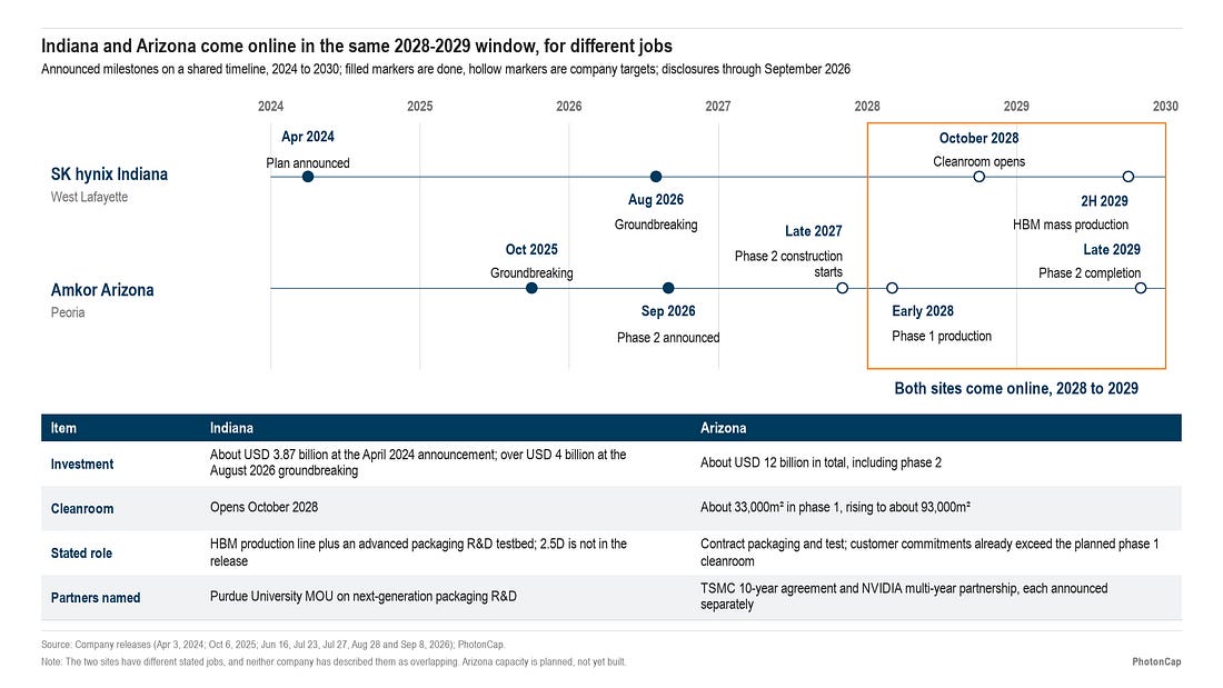
Indiana and Amkor Arizona come online in the same 2028-2029 window but for different jobs. Shared timeline with investment, cleanroom, role and partner comparison
Equipment. At the end of June, Hanmi Semiconductor released the FC Bonder 3.5. It bonds 2.5D logic dies chip-to-wafer (C2W), can handle large panels and substrates up to 340mm, and also supports multi-die processes based on panel level packaging (PLP) [18]. Then at SEMICON Taiwan in early September it showed five 2.5D tools at once, from the FC Bonder 3.5 and 75 to the 2.5D TC Bonder 40 in C2S (chip-to-substrate) and C2W versions and the 2.5D TC Bonder 120. The four other than the 120 have been launched one after another since late last year and are reportedly being supplied now for volume production to global foundries and OSATs (outsourced assembly and test companies), while the 120 is about to launch [19]. The reason I’m paying attention to the part about the FC Bonder 3.5 handling 340mm substrates is that, if the in-house 2.5D grows toward large-area packages, I think bonders are likely to be the first equipment it needs. A company whose main product is the HBM TC bonder has already set foot in large-area 2.5D as well.
Materials. The item to watch here is the silicon capacitor. On May 20, Samsung Electro-Mechanics filed a single sales and supply contract disclosure on DART, Korea’s electronic disclosure system. The counterparty is listed only as “a large global company,” and following a request to protect trade secrets, the counterparty and the main terms will be disclosed on the business day after the deferral deadline. The contract is worth 1.557 trillion won, which is $1.0354 billion converted at 1,503.80 won per dollar, the first base exchange rate posted on the contract date. That comes to 13.8% of consolidated revenue for 2025, the contract runs from January 1, 2027 to December 31, 2028, and the disclosure is deferred until December 31, 2028 [20]. The filing names it a “Silicon Capacitor supply contract,” and the body of the filing doesn’t say what it’s for. A Samsung Electro-Mechanics press release the same day described it as a part that goes inside high-performance semiconductor packages, such as GPUs and HBM for AI servers, to make the power supply more stable. It’s an ultra-small capacitor built on a silicon wafer, a different product from the MLCC (multilayer ceramic capacitor) that is Samsung Electro-Mechanics’ main business, and the company says its ESL and ESR (the part’s own parasitic inductance and resistance) are more than 100 times lower than an MLCC’s [20].
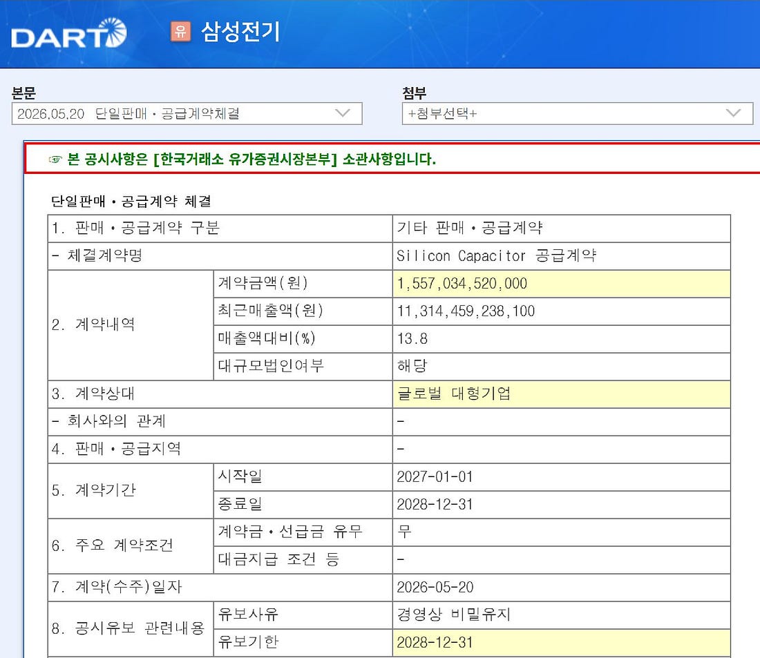
Key fields of Samsung Electro-Mechanics’ single sales and supply contract filing (May 20, 2026, receipt no. 20260520800239). Source: DART
Some brokerage reports name a specific product of a specific customer as where this contract ends up, but that’s only an estimate, and the filing doesn’t disclose the counterparty. I won’t narrow it down any further either. Still, a contract this large for silicon capacitors alone looks to me like a sign that power stabilization inside large-area packages has become homework for the whole industry. Besides Samsung Electro-Mechanics, Murata (TSE:6981) has been in the silicon capacitor business since it acquired IPDiA in 2016 [21], and Kyocera, Vishay, STMicroelectronics, Rohm and Skyworks are also known to make silicon capacitors.
To be clear about one thing: none of Samsung Electro-Mechanics, Murata or Kyocera has been confirmed as a DTC supplier for SK hynix’s in-house 2.5D at this point. The speaker only said it’s being developed with the company’s research institute and didn’t say who manufactures it, so we don’t know whether it’s even sourced from outside. The companies listed here sell into this area, and this shouldn’t be read as a list of SK hynix suppliers.
Intel’s EMIB-T. Intel is the company solving the same problem a different way. EMIB-T first appeared in a paper at ECTC 2025, and Intel showed expanded results at ECTC 2026 in late May this year. The T stands for TSV. TSVs drilled through the bridge carry power coming up from the bottom of the package through the bridge to the HBM. According to Intel’s blog, bump pitch has been brought down to 25μm and packages have grown to 120mm on a side [22]. The figure that DC voltage drop falls by roughly 70-80% appeared as Intel’s claim in SemiAnalysis’s review of ECTC 2026 [23], and a roadmap for packages 180mm on the long side carrying 38 or more bridges, along with a figure of 24 or more HBM stacks, came from reports on roadmap slides [24]. Here it helps to separate what each part does. Intel’s bridge TSVs are a vertical path for power (signals still run horizontally through the bridge’s wiring layers, as before), and MIM (metal-insulator-metal) capacitors inside the same bridge suppress AC noise. The DTC in the bridge that SK hynix talked about stores charge locally to damp sudden changes in current, so on Intel’s side the part playing a similar role is the MIM capacitor rather than the TSV. TSMC’s CoWoS-L deals with the same problem using stand-alone eDTC under the SoC and eDTC inside the LSI bridges. So the three companies are each solving the same problem, power integrity in large-area 2.5D packages, with a different part.
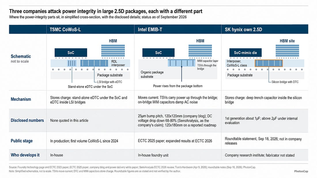
Three companies attack power integrity in large 2.5D packages with different parts. Simplified cross-sections with mechanism, numbers, stage and developer comparison
Substrates. As large-area 2.5D gets bigger, the substrate becomes a problem too. In February 2026, the board of Ibiden (TSE:4062) approved a plan to expand high-performance IC package substrate capacity by a total of about 500 billion yen over FY2026-FY2028. Phase 1, about 220 billion yen, goes into existing plants such as the Gama plant, and phase 2, about 280 billion yen, is centered on the Ono plant, with operations starting in stages from FY2027. This is a total investment plan approved by the board, so it should be kept separate from the money actually spent so far [25]. Unimicron (TWSE:3037) also raised its 2026 capex in February to a record NT$34 billion (about $1.1 billion), and about 70% of that was for ABF (Ajinomoto build-up film) substrate capacity and process upgrades. AI is expected to pass 60% of its revenue in 2026 [26]. At its July 29 board meeting it raised capex again, to NT$53.7 billion (about $1.7 billion), and said it would put more than 80% of the increase into ABF substrates [27]. Shinko Electric Industries, often mentioned alongside Ibiden and Unimicron, was acquired by a JIC consortium and delisted in June 2025 [28]. So of the three compared in this piece, the ones you can reach directly as listed stocks are Ibiden and Unimicron.
While Indiana is being built, customer commitments at Amkor Arizona filled up ahead of its planned capacity. Bonders and silicon capacitors are already moving toward large-area 2.5D. Intel is working on the same problem through the bridge power path, and on the substrate side three-year expansion plans have been approved. Whether the in-house 2.5D becomes a business or stays a validation tool, if that line gets built, this supply chain could gain one more source of demand. It’s the multi-foundry trend I covered in The GPU era ran on TSMC. The inference era runs on multiple foundries: NVIDIA Rubin NVL8 and 14 stocks, showing up in a similar way on the packaging side.
Moving this over to investments, the exposure confirmed by public material is Amkor’s contract expansion in the US, Hanmi Semiconductor’s supply of 2.5D bonders for volume production, Ibiden’s and Unimicron’s substrate expansion, and Samsung Electro-Mechanics’ large silicon capacitor contract. On the other hand, no company has been confirmed to have a supply relationship with SK hynix’s in-house 2.5D line, and the line has no revenue of its own yet. So the signals to watch from here are order filings, customer qualification, and the timing of equipment move-in at Indiana. I’d add that the value of this line is more likely to come from cost savings than from new revenue. Screening out HBM failures in customers’ packages ahead of time cuts redesign and RMA handling costs, and on the income statement those savings show up on the cost side rather than as revenue.
The TSMC relationship. If the in-house 2.5D line goes up, the bridge DTC is developed in-house as well, and validation runs at the Indiana testbed, will it really end up colliding with TSMC? As you may have guessed, the speaker’s answer was that it won’t. On the Indiana question, the answer was that they’re preparing technically so there’s no IP conflict, and that it’s a model that grows the whole market pie instead of trying to monopolize it, within limits that don’t affect a strong partner. The speaker added that the market can’t grow if TSMC can’t handle it all. On whether the relationship had gone bad, the speaker said technology and products have to be looked at separately. Technology used in logic has eventually come over to memory, with a lag of a few years at the short end and close to 20 years at the long end, and transistors are no exception, so there’s reason to develop logic transistors, but that’s no reason to break the HBM base die ecosystem. All of this comes from the speaker’s remarks and doesn’t represent an official company position.
7. Closing
The conclusion of this piece is short. Going by what was explained at the event, the current priority of the in-house
- 5D is to find out firsthand under what conditions the company’s HBM fails inside customers’ packages, and the place to
do that work is the R&D testbed in Indiana. What I heard in the room, that R&D capacity in Taiwan is concentrated on big customers and second-tier players and startups struggle to find room, supports the second reason to exist, but whether it grows into a packaging business for outside customers is a separate question. Answering that means watching whether customer qualification and the scope of the service take concrete shape, and what has come out so far goes only as far as trying tests with a few interested customers.
If the CoWoS supply gap narrows faster than reported (from 20% to 10% by the end of 2026), and second-tier players stop saying they can’t get R&D capacity in Taiwan, the second reason to exist weakens accordingly. On the other hand, if the company announces, from the moment the Indiana testbed opens, that it’s offering the in-house 2.5D as a contract service for outside customers, then this piece’s call that validation comes first was wrong from the start. If revenue starts coming in with named outside customers after the validation line has run for a few years, I’ll read that as the move into commercialization happening in the expected order. There are also a few dates to check. At TSMC’s third-quarter call on October 15, look for comments on CoWoS capacity; at Intel’s results on October 22, external EMIB customer orders; and at SK hynix’s third-quarter call on October 27, questions about Indiana’s purpose and 2.5D (none of the three dates had been officially announced by the companies as of September 21, so they may change). After those come the Indiana cleanroom opening in October 2028 and production in the second half of 2029. I’ll keep checking in this series what goes off track in between.
8. References
[1] wccftech: SK Hynix Unpacks Advanced Packaging Technologies, Including Intel EMIB, For Its Next-Gen HBM Memory, 2026-08-23 · ServeTheHome slides
[2] Digital Daily: SK hynix says hybrid bonding and 3D packaging are the core of future competition (in Korean), 2024-08-27
[3] ZDNet Korea: SK hynix moves to build its first 2.5D packaging production line in the US (in Korean), 2025-12-29
[4] ZDNet Korea: SK hynix pursues 2.5D packaging cooperation with Intel (in Korean), 2026-05-11
[5] SK hynix Newsroom: Groundbreaking Ceremony for HBM Production Base in Indiana, 2026-08-28 · 2024-04-03 investment announcement
[6] TSMC 3DFabric: CoWoS technology page, retrieved 2026-09-23
[7] IEEE ECTC 2023: CoWoS Architecture Evolution for Next Generation HPC on 2.5D System in Package (TSMC)
[8] Tom’s Hardware: TSMC details next-gen CoWoS roadmap, over 14-reticle packages expected by 2029, 2026-04-27
[9] Tom’s Hardware: TSMC’s ‘Super Carrier’ CoWoS interposer gets bigger, 2024-11-27
[10] TrendForce: TSMC Targets CoWoS With 24 HBM Stacks in 2029, 2026-05-14
[11] TrendForce: TSMC CoWoS Supply-Demand Gap Reportedly Seen Narrowing from 20% to 10% by End-2026, 2026-06-15
[12] TrendForce: TSMC Reportedly Targets 22% 2nm Capacity Boost by Mid-2027; CoWoS to Double by 2028, 2026-09-14
[13] SK hynix Newsroom: SK hynix Indiana fab breaks ground as new hub for US AI innovation, 2026-08-28
[14] Amkor: Phase 2 of Arizona Advanced Packaging and Test Campus, 2026-09-08 · 2025-10-06 groundbreaking announcement
[15] Amkor: Financial Results for the Second Quarter 2026, 2026-07-27 · Earnings call transcript
[16] Amkor: TSMC and Amkor Technology Announce Long-Term Partnership, 2026-06-16
[17] Amkor: Strategic Partnership with NVIDIA to Expand U.S. Advanced Packaging Capacity, 2026-07-23
[18] Etoday: Hanmi Semiconductor launches ‘FC Bonder 3.5’ for AI system semiconductors (in Korean), 2026-06-26
[19] Digital Daily: Hanmi Semiconductor unveils a range of 2.5D packaging equipment at SEMICON Taiwan 2026 (in Korean), 2026-09-02
[20] Samsung Electro-Mechanics: Single sales and supply contract (DART filing, in Korean), 2026-05-20 · Company IR disclosure · Newsroom press release (in Korean)
[21] Murata: Closed the acquisition of IPDiA, a leader in high performance silicon capacitors, 2016-10-18
[22] Intel Foundry: How Intel Foundry Packaging Technologies Redefine AI and HPC Scalability Limits at ECTC 2026, 2026-06-02 · ECTC 2025 EMIB-T paper · Power delivery white paper, 2026-08
[23] SemiAnalysis: ECTC 2026 review, 2026-07-02 (secondary source)
[24] Tom’s Hardware: Intel’s EMIB-T heads for fab rollout this year, 2026-04-09 · wccftech, 2026-04-30
[25] IBIDEN: Notice Regarding Capital Investment Plan for High-Performance IC Package Substrates, 2026-02-03 · 2026-02-26 Disclosure Update
[26] Taiwan News: Unimicron 2026 capex and AI revenue share, 2026-06-01 · MoneyDJ (in Chinese), 2026-06-05 · DigiTimes, 2026-02-25 (paywalled)
[27] TechNews: Unimicron raises 2026 capex to NT$53.7 billion (in Chinese), 2026-07-29
[28] JPX: Decision to delist Shinko Electric Industries, 2025-05-20 · JIC acquisition announcement
This article is an independent technical analysis published by PhotonCap, based on an engineering perspective. All content is derived from publicly available information and the author’s on-site notes, and remarks heard at the event are identified as such in the text. It is intended solely for educational and informational purposes. In other words, nothing in this material should be construed as a recommendation to buy, sell, or hold any specific securities. Please note this carefully.
The author may hold positions in the securities mentioned herein and reserves the right to trade such securities at any time without prior notice. Readers should conduct their own thorough review and research before making any investment decisions.
Share this with anyone who needs to see the world through a different wavelength.
Share