2026.09.30 | Substack | Memory | Micron HBM Speed Expert Call
原标题:[Expert Call Report] How Is Micron Making HBM Faster?
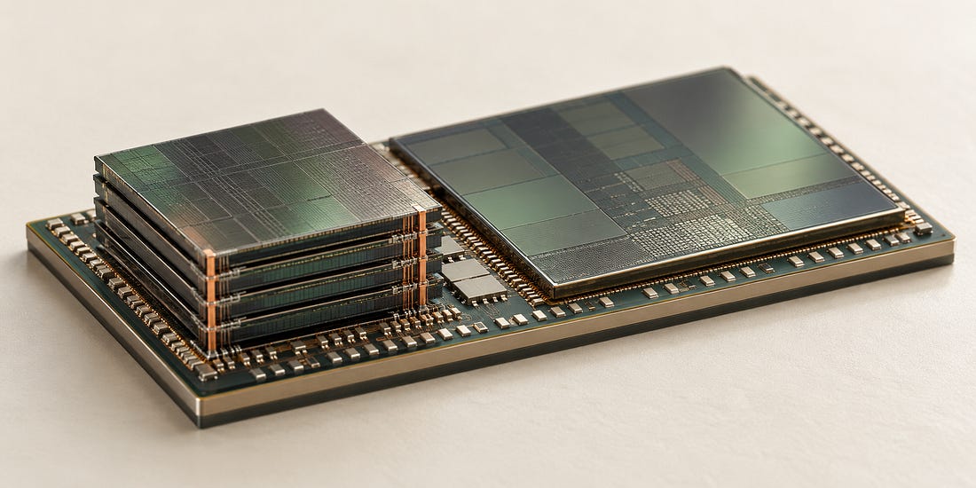
The importance of HBM bandwidth is now familiar. But what has to change inside HBM to make each pin faster? I wanted to understand whether a faster logic process would be enough, whether more TSVs were needed, and how the DRAM stacked above the base die could keep up.
The expert I spoke with designs HBM interfaces at Micron. After working on high speed interface design at Samsung, he moved to Micron, where he now works on both sides of the HBM base die: the interface to the GPU and the interface to the DRAM core dies. Our conversation began with the circuits that transmit and receive signals, then moved into bandwidth and heat in future HBM generations, custom designs, and architectures that stack memory directly on top of a compute chip.
What stayed with me most was how my own question had changed by the end of the conversation. I began by asking what it would take to make HBM faster. As we went on, I became more interested in who would design each part of this increasingly complex memory, and who would capture the value.
I had assumed that bringing memory and logic closer together would naturally expand the role of memory companies. The expert pointed to another possibility. If customers take on more of the logic and interface design, memory companies could end up with a narrower design role even as stacking technology advances. The Q&A below preserves the explanations and followup questions that led me to that realization.
KEY TAKEAWAYS
1. Pin speed is also a problem inside the DRAM.
Distributing incoming high speed data across more internal paths running at lower speeds can ease the demands on DRAM. The cost is more TSVs, more routing, more area, and greater expense.
2.Future HBM makes both receiving and routing harder.
Higher pin speeds increase channel loss and make signals harder to distinguish. If DRAM speed remains unchanged, the design must also accommodate more parallel paths.
3.Fewer layers do not tell the whole capacity story.
Electrical loading, supply conditions, and each customer’s product configuration all matter. Requests for fewer layers do not, by themselves, mean that the need for taller stacks has disappeared.
4.Progress in 3D stacking does not guarantee design control.
Reducing external connections does not eliminate the need to reconcile the speeds of logic and DRAM. If customer specific TSV layouts also require changes to the core die, design reuse and staffing become additional concerns.
The questions and answers have been organized by topic from the original recording. Repetition and personal conversation have been removed; this is not a verbatim transcript. The context distinguishing the expert’s experience, information heard from others, and personal reasoning has been preserved. The answers do not represent the company’s official position. Explanations added beyond the interview are labeled “Editor’s note,” and the interviewer’s analysis is labeled “Damnang’s take.”
Generative AI assisted with editing and the creation of visual material.
Damnang Research is a reader-supported publication. To receive new posts and support my work, consider becoming a free or paid subscriber.
 Subscribed
1. HBM has two distinct interfaces
Damnang
Could you start by briefly introducing the work you do?
Expert
I design HBM at Micron, specifically the interfaces. An interface enables chips to exchange signals reliably. Our job is to transmit clean signals, receive them without errors, interpret the incoming analog signals as digital data, and pass that data into the chip.
I specialized in high speed interface design during my PhD and also worked on SSD interface design at Samsung. I later moved to Micron, where I now design HBM interfaces.
Damnang
When you say interface design, what kinds of circuits do you work on?
Expert
The circuit that sends a signal is called the transmitter, or TX, and the one that receives it is called the receiver, or RX. Suppose we need to send four parallel data streams from inside a chip. We could send each one out separately, but getting signals out of a chip is itself a challenge. Each I/O consumes substantial power, and the hardware needed to implement it is costly.
So we combine the parallel data into a faster serial stream, transmit it, then sample the signal at the receiving end and expand it back into multiple parallel streams. The circuits that perform those functions are the serializer and deserializer, collectively called SerDes.
Signals also become distorted as they pass through a channel. That channel might be a PCB, or a silicon interposer in the case of HBM. An equalizer compensates for signal distortion according to the characteristics of the channel. Interface design covers this serialization, deserialization, and signal compensation.

Damnang
So is it fair to say that you currently develop SerDes and equalizers for the HBM base die?
Expert
Yes. But with HBM, you have to think about the interface in two directions. One connects the base die to the GPU through the interposer. The other connects the base die to the DRAM core dies above it through TSVs.
The interface to the GPU and the TSV interface to the DRAM have different characteristics. I work on both.

Damnang
What is the main technical difference between the two?
Expert
First, the channel characteristics are different. The interposer connection runs outside the chip, and signal distortion increases as the path gets longer. It also operates at a higher speed. You therefore have to design the transmitter, receiver, and equalizer to suit that channel.
By contrast, the connection to the DRAM above does not have to carry data at the same speed as the external input. It can split the data across more paths and transfer it at a lower speed. Even though both sides carry the same data, they do not operate under identical conditions.
Editor’s note | What SerDes means in this article
Here, SerDes refers to the functions that serialize and deserialize data within the interface circuitry. It does not mean that HBM as a whole is a single serial link. Many data I/Os run in parallel between the GPU and HBM, so the speed of each I/O must be distinguished from the width of the internal data path.
2. Faster pins require more internal data paths
Damnang
So the external pin speed can differ from the speed of the internal TSVs. Could you walk us through a numerical example?
Expert
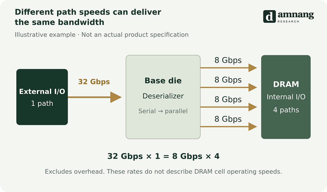
Suppose data comes in through a single DQ pin at 32 Gbps. If we split that input across four internal paths, we can have four paths operating at 8 Gbps each. We receive data at high speed from outside, then use more paths internally to reduce the speed required of each one.
I have chosen these numbers and ratios purely as an illustration. The ratios that individual companies actually use are a separate question.
Damnang
So each TSV carries data at a lower speed, but you need more TSVs?
Expert
Exactly. For example, if there are 1,024 external data paths and we split each one into four, we would need roughly 4,000 paths inside. Lower speed comes at the cost of more connections, so there is a balance to strike.
JEDEC standards define things like the interface and commands used to communicate with the customer’s device. They do not require everyone to use the same ratio internally. From the customer’s perspective, what matters is being able to read and write data when needed. The memory vendor can decide how to implement that internally.
So I do not know whether Samsung, SK hynix, and Micron use the same ratio. They could be different.
Damnang
Even if the HBM meets the same standard, the implementation can differ depending on the internal SerDes architecture and the number of TSVs chosen.
Expert
Yes. Those are the decisions we make in advanced development. We look at whether four to one is better, whether eight to one makes sense, or whether we should go as far as sixteen to one.
Splitting the data across more paths allows the DRAM to operate at a lower speed, but too many TSVs can increase manufacturing costs and design complexity. Our work involves finding that balance and defining the architecture for the next generation.
Damnang’s take
It is easy to miss this point if we assume that HBM’s external pin count and internal TSV count are the same. Increasing the number of internal paths while maintaining external bandwidth reduces the speed required of each path. The key is choosing the right balance between DRAM operating margin, routing, die area, and cost, rather than simply adding as many TSVs as possible.
3. Why a better logic process is not enough
Damnang
Is the main reason for splitting the data that the DRAM dies above cannot easily receive it at the original speed?
Expert
Exactly. A base die built on a logic process is different from the DRAM dies above it. From the perspective of high speed circuitry, the DRAM does not have the same characteristics. If you send the fast external data straight up to the DRAM, the receiver may not be able to sample it at that speed. Timing mismatches can then lead to incorrect reads or writes.
So you have to split the data until each path operates at a speed the DRAM can handle. That is also why you cannot simply keep reducing the number of internal paths. The DRAM I/O becomes one of the bottlenecks.
Damnang
Then the process used for the base die must matter too. A more advanced logic process should help it receive faster external signals and distribute the data internally.
Expert
It does play a role. The core dies have to support the design, but the base die also needs to handle that speed. If the base die receives the data at high speed and distributes it across enough paths, the DRAM can receive it at a speed it is capable of handling.
That said, if you look at high speed logic interfaces in isolation, other fields already handle signals much faster than the pin speeds discussed for HBM. The SSD designs I worked on were an example. So with HBM, you cannot look only at the base die’s speed. You have to consider how it works when connected to the DRAM above it.
Damnang
When I was studying Samsung’s HBM papers, I noticed not only the transition to a logic process but also the higher TSV count. Could that be an important clue to how they increase bandwidth?
Expert
A higher TSV count can be a clue. One possible interpretation is that they increased the deserialization ratio to give the DRAM dies more margin to operate reliably at a lower speed.
How Samsung Overtakes SK hynix in HBM4: An ISSCC 2026 Paper Review
Damnang
·
Mar 20
Read full story
Damnang
I see. So increasing pin speed is not just a matter of making the logic die faster. The connected DRAM also has to be able to receive the data.
Expert
Correct. You need deserialization to bring the speed down to a level the DRAM can handle.
Damnang
I had heard that even meeting the existing speed targets was difficult, so I was surprised to see higher speeds being discussed so soon. Can major design changes make that possible?
Expert
It can be difficult if you are trying to increase speed while keeping the existing design. But if you change enough of the design, it may be possible. Raising the speed a little within the same architecture and reworking the architecture are two different problems.
Editor’s note | Comparing data rates across interfaces
The expert’s experience with higher data rates in other interfaces provides context for what logic processes can support. It is not a direct performance comparison between PCIe and HBM, which differ in signaling, channel characteristics, I/O count, and power budget. Gbps in this article refers to the bit rate of a pin or data path, distinct from the bandwidth of an entire stack expressed in bytes per second.
Editor’s note | Micron’s base die transition
In its September 2025 earnings materials, Micron said it uses its own advanced CMOS base die for HBM4 and will work with TSMC to manufacture the base logic die for both standard and custom HBM4E. The presence of a base die must therefore be distinguished from the transition to a logic process at an external foundry. The discussion of Samsung’s TSVs above is also an inference from a design perspective, not a statement based on confirmation of the actual internal design.
4. HBM5 makes signal reception and routing harder
Damnang
You mentioned that you have now moved on to the next generation of HBM. Looking toward HBM5, what becomes most difficult on the interface side?
Expert
First, the speed increases. We can consider a case where the external pin speed rises from around 16 Gbps to around 32 Gbps. But I think it would be difficult for the operating speed of the DRAM die to double in a single generation.
A DRAM process is optimized to reduce leakage current and build the cells and capacitors that store data. That is a different direction from optimizing transistors for high speed logic circuits. So, if we assume that the speed on the DRAM side stays roughly the same, doubling the external speed means doubling the internal deserialization ratio. The number of paths leading to the TSVs increases accordingly.
Damnang
So this is more than making a receiver circuit faster. The connections behind it also change substantially.
Expert
Exactly. You need that many more wires running from the deserializer to the TSVs. Managing that routing becomes harder, and you have to rethink the architecture.
At the same time, losses on the external interposer increase as the speed rises. The signal may already be in worse shape by the time it reaches the receiver. You have to expand the internal parallel paths while also receiving a faster external signal reliably.
Damnang
When you say the signal deteriorates, do you mean it becomes harder for the receiver to distinguish a 0 from a 1?
Expert
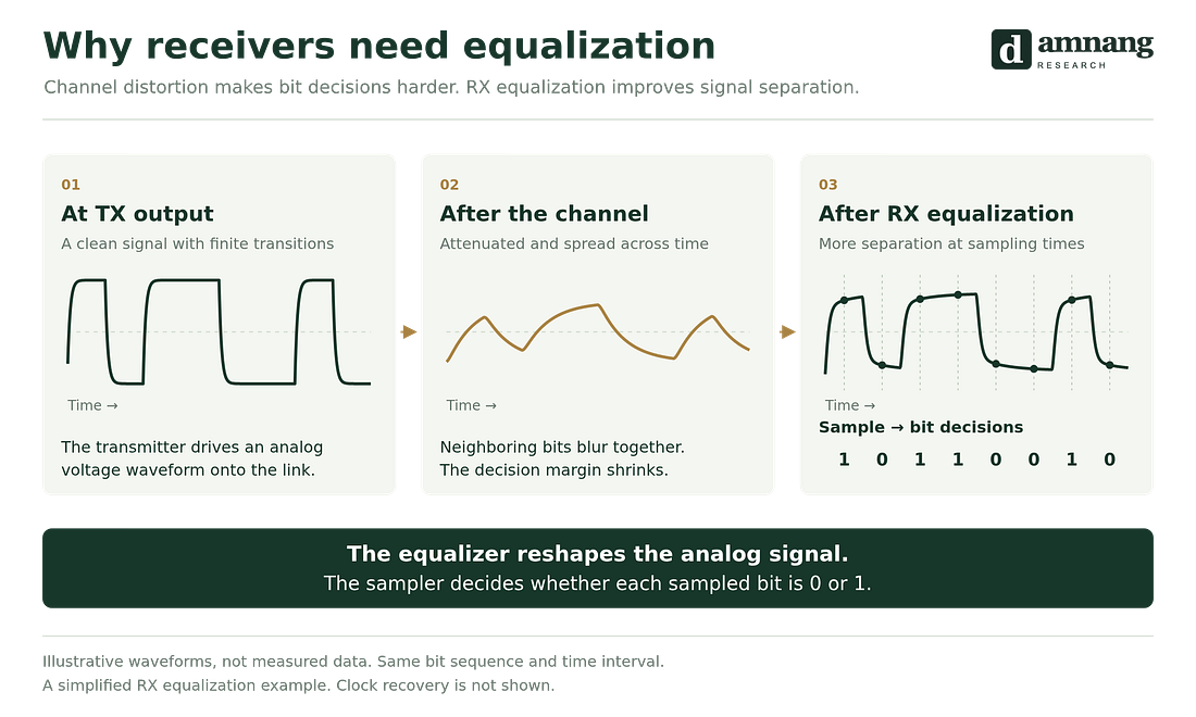
Yes. Even if the transmitter sends clean 0s and 1s, the waveform spreads out as it passes through the channel, and noise and other forms of distortion are introduced. The receiver has to decide that a signal above a certain threshold is a 1 and a signal below it is a 0. As channel conditions deteriorate, making that distinction at the sampling instant becomes more difficult.
You need an equalizer to compensate for the signal degradation so that you can distinguish between them again. As the speed increases further, the problem becomes more severe and places a greater burden on the receiver circuit.
Damnang
You also mentioned that the work is increasingly becoming almost like custom development. Is that connected to the speed requirements?
Expert
Large customers do not just look at the speeds in the standard. They ask for the speeds they need. When they say, ‘We need this speed,’ we work toward it. My sense is that, as we move forward, the work is increasingly taking on the character of custom development around customer requirements, rather than simply developing standard products.
But speed is not the only difference with custom HBM. The logic placed on the base die can change, as can who implements the interface and how they implement it.
Editor’s note | Standards and the speed targets discussed
The 16 Gbps and 32 Gbps figures in this section provide a comparison for the future design directions discussed in the interview. They do not represent finalized standards for HBM4, HBM4E, or HBM5, or the specifications of any particular product in volume production.
The initial HBM4 standard, announced in April 2025, specified an interface 2,048 bits wide, speeds of up to 8 Gb/s per pin, and bandwidth of up to 2 TB/s per stack. Micron’s public HBM4 product page, meanwhile, lists more than 11 Gbps per pin and more than 2.8 TB/s per stack. The figures in the initial standard, actual product specifications, and future design targets should be read as distinct categories.
Damnang’s take
It is easy to underestimate the challenge if we think only about external pin speed doubling. If the DRAM side does not improve at the same rate, the design has to receive a more difficult signal while also expanding the internal paths. The challenges of developing the next generation of HBM compound across the receiver, speed conversion, TSVs, and routing.
5. Custom HBM changes how the base die is designed
Damnang
With custom HBM, does the change go beyond adding circuits to meet the pin speed requirement? Does the composition of the base die itself change?
Expert
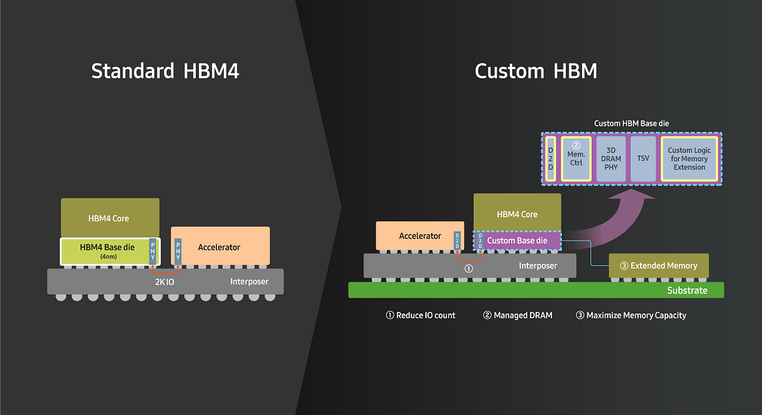
Some circuits may be needed for speed, but the bigger difference is that the customer’s logic moves onto the base die. That could include a memory controller or some basic compute functions.
With a standard product, we have some room to choose the internal deserialization ratio, the equalizer, and the RX architecture. But once customer logic is included, it also constrains how much area the interface can use. The entire base die has to be designed together.
Source: https://semiconductor.samsung.com/foundry/application-specific-service/hpc-ai/
Damnang
Does that also mean greater use of interfaces as IP blocks?
Expert
Yes. One possible direction is to use specifications and IP such as UCIe. If both ends of the connection follow an agreed protocol, customers can design around it, and it also becomes easier to manage on the memory side.
Using a foundry logic process also gives you access to a much broader range of IP. You can bring in external IP or use something developed internally, but that changes the nature of the work compared with the traditional approach of designing the interface directly within the memory company.
Damnang
From an interface designer’s perspective, could custom HBM actually make it easier to improve performance in some respects?
Expert
From our team’s perspective, there could actually be no work left for us in that part of the design. If the external interface is implemented using other IP or handled by someone else, the role I used to perform changes. It is not simply a matter of the design becoming easier.
Damnang
I see. Custom HBM could create more work while also shifting some of the design responsibilities you used to have to someone else. That also makes me wonder whether memory companies gain more control over the base die, or whether their role becomes implementing what the customer asks for.
Expert
I review the custom HBM work rather than being directly responsible for it, so I cannot give a precise account of the whole picture. But there seems to be a great deal of discussion with customers as the two sides work to align their designs. There are interconnected areas such as the memory controller, I/O, and TSV region.
From what I can see, NVIDIA seems inclined to take on a large share of the design itself. NVIDIA already has experience with very fast interfaces in other areas. There is a difference in starting point: the memory side is moving up from relatively low speeds, while NVIDIA approaches this with experience at higher speeds.
That does not mean everyone views this only with discomfort. Ultimately, the product has to be built, so each side works out which parts it will handle.
Damnang
When I looked at the discussion around NVHBM, I felt that NVIDIA was trying to define a common form of custom HBM around its own requirements. I thought that giving all three memory suppliers the same requirements could also affect price negotiations.
Expert
That is one way to look at it. You could also see it as a change in the customer’s role. The comparison I hear from people around me is that Intel used to sit in the middle, coordinating multiple memory suppliers and helping lead the standards process. NVIDIA today seems much more focused on fitting everything to its own ecosystem.
Developing around a customer’s requirements also raises considerations for the memory company. If all you have is a design tailored to one customer, it may be difficult to use elsewhere. So it could be more efficient to manage the remaining portions as reusable IP, apart from the parts that contain the customer’s own IP.
Damnang
If you package those functions as IP, you could use the same assets for other customers. You could also tell them, ‘These are the functions and specifications we can offer.’
Expert
Exactly. But you should not take that to mean we are doing this because we are worried about being left with unsold inventory that has already been produced. In the context I am describing, the bigger purpose is to reduce the strain on designers and the staffing burden. It reduces the need to build everything from scratch for each customer.
Editor’s note | UCIe and customer specifications
UCIe stands for Universal Chiplet Interconnect Express, an open specification for connections between chips within a package. It was mentioned here to illustrate an approach to managing interfaces through specifications and IP. The discussion does not confirm its adoption in any particular HBM product from any particular company. The interpretation of NVHBM’s implications for price negotiations should be understood as part of Damnang’s question.
6. How Micron is building its HBM capabilities
Damnang
Having worked at Samsung and now at Micron, you probably notice differences in how the companies compete. Are there areas where Micron does particularly well or takes a different approach?
Expert
I did not work directly on HBM at Samsung, so it is difficult for me to make a precise comparison between the two HBM organizations. But comparing what I have heard with what I have seen here, there seems to be a difference in how they bring in talent.
I heard that when HBM became important, Samsung responded by pulling people from different departments to form a task force. That can concentrate capabilities on an important project, but the teams supplying those people still have their own work to do, so it can put pressure on them.
At Micron, I saw very aggressive hiring of experienced engineers when the company needed to expand its HBM capabilities quickly. It kept bringing in experienced people from other memory companies to grow the organization. The approach leaned more toward hiring externally than taking people from existing teams and leaving gaps behind.
Damnang
That sounds effective for quickly acquiring the capabilities you need right away. Are there drawbacks to that approach?
Expert
You can end up with an inverted pyramid, with many senior engineers and relatively few junior staff. Hiring a lot of experienced people helps you move quickly in the short term, but that structure is difficult to sustain over the long term.
That is why there is now talk of needing to hire many more new graduates as well. Bringing in the experience needed today and developing the workforce for the future have to happen together.
Damnang
I imagine there is also considerable pressure from customers comparing suppliers and demanding higher speeds.
Expert
Our department does not interact directly with customers. But judging from what the people who do meet customers share in working groups, there does seem to be some comparison of where each competitor stands.
The pressure can also vary by team. The volume production side has immediate requirements to meet, while teams working on advanced design focus on longer term challenges. I cannot take what I see and present it as the experience of the entire production organization.
Damnang
As designs mature and customer specifications become clearer, that could create opportunities for Micron as it works to catch up. Of course, volume manufacturing and process competitiveness are separate questions.
Expert
I think that is possible. You could see opportunities from that perspective.
Damnang’s take
This conversation provided insight into which capabilities Micron is building to catch up, and how it is building them. It did not establish that Micron will ultimately win. Hiring experienced engineers to acquire design expertise immediately and developing the workforce needed to sustain an organization are distinct challenges. Progress in interface design also does not, by itself, tell us about production yields or customer qualification.
7. Are 8 or 4 layers just a question of capacity demand?
Damnang
One area I have been following closely is the number of layers in a stack. It seemed we would keep moving toward 12 or 16 layers, but I am also hearing about requests for 8 layers or even fewer. How do you see that trend?
Expert
When I first heard about 8 layers, I also wondered whether it was because of poor yields in bonding or other processes. But the explanation I heard later was about customer segments and the product mix.
Some customers who want standard products do not need extremely large capacities. The explanation was that we need to distinguish between customers who want custom products with more layers and customers who want standard products that provide the capacity they need. If there are not enough customers to buy a standard product with more layers, it makes more sense to build the layer count that fits that customer group.
That was the context relayed to me. Hearing about fewer layers was not, by itself, a reason to jump to the conclusion that there was a process technology problem.
Damnang
By a standard product, you mean a case where the customer designs its chip to the JEDEC specification and connects it to HBM, correct?
Expert
Yes. For a smaller company to jointly develop a custom die, it needs more people and ongoing communication to align the designs. That is a substantial burden.
With a standard product, however, the customer can design its side to a defined specification. It wants to connect and use a predefined product, as it would with conventional memory. Standards serve a purpose for those customers as well.
Damnang
But some of the requests for fewer layers that I heard about came from large customers. Can demand for standard products explain all of those cases too?
Expert
I do not know whether those requests were for standard products. My understanding was that large customers wanted large capacities. But connecting that with what I had heard in conversations in the field, I think we also need to consider supply.
For example, if building stacks with more layers makes supply more difficult, a customer might choose to use more stacks with 8 layers instead. But that is an inference I am making from what I have heard, not something I am saying with precise knowledge of that customer’s plans.
Damnang
That is exactly what I was wondering about. When the layer count falls, one interpretation is that AI may not need as much HBM capacity as people expected. On the other hand, there is also the view that larger workloads will lead back to stacks with more layers.
Expert
That demand strategy is outside what I can assess, since I work on circuit design. But I can explain the conditions we consider when designing.
We design the TSV interface between the base die and the DRAM for the worst case, assuming a stack with a high layer count. For example, stacking 12 or 16 layers increases the load and capacitance, making channel conditions worse. The interface has to work under those conditions too.
If we designed for 4 layers just because we heard that was what would be used now, it would be difficult to respond later if 8 or 12 layers were needed. That is why we use the more demanding conditions as our design basis.
Damnang
In that case, reducing the number of layers could improve the electrical conditions. Could that create options to increase speed or reduce the deserialization ratio?
Expert
It could. A lower load can give you more margin. At that load, you might consider operating faster or using a lower deserialization ratio. But it depends on the architecture you choose.
Damnang
Then choosing the layer count involves interface conditions and supply as well as capacity. Other DRAM products also need production resources, alongside HBM.
Expert
Exactly. Production considerations seem to come into it as well, beyond the technical issues.
Damnang’s take
The important distinction in this section is that a request for fewer layers and a reduction in total memory capacity needs are not the same observation. We have to consider the customer segment, the number of stacks deployed, supply conditions, and the electrical conditions of the interface together. The expert explained the design margin that fewer layers might create. The expert did not confirm a decline in demand from any particular customer or a future roadmap for layer counts.
8. Does stacking memory on compute eliminate SerDes?
Damnang
Let’s take this a step beyond custom HBM. Instead of placing HBM beside the GPU, 3D stacked DRAM puts memory directly on top of the compute die. How do you see that from an interface perspective?
Expert
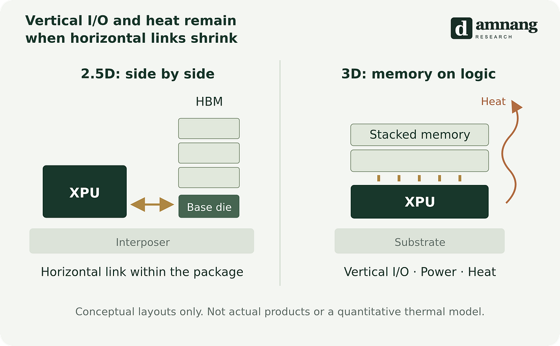
Logically, I think it is a natural direction. Today, logic and memory sit beside each other and connect through a 2.5D structure. If you can stack them vertically, you can connect them more directly.
From an interface perspective, the connection that used to run outside the chip goes away. In my role, the focus shifts to the vertical TSV interface, which can reduce some of the design burden associated with the conventional external interface.
But heat is still a problem. Removing heat from a stacked structure is difficult, and a compute die such as an XPU underneath it can generate even more heat. As speeds continue to rise, I think heat could become the limiting factor first.
Terminology | 3D stacked DRAM in this article
Here, the term refers to vertically integrating DRAM dies with compute logic. That is a different discussion from the process technology for ‘3D DRAM,’ in which the DRAM cell structure itself extends across multiple layers.
Damnang
So if we stack the dies in 3D, does that remove the need for SerDes?
Expert
It is hard to say the need disappears entirely. Logic runs fast and wants to exchange data with memory quickly. But DRAM cannot operate at the same speed as that logic.
You still need a function in between that distributes the data across parallel paths and matches their speeds. Removing the conventional external connection does not remove the speed difference between logic and DRAM. You also still have to decide what ratio to use when dividing up the data.
Damnang
I see. You reduce the portion of the connection that goes out through the interposer, but you do not eliminate the speed conversion in the internal interface to the DRAM.
Expert
Right. That function still has to be there. Choosing the ratio then becomes a design question again.
Damnang
When I heard this structure explained by people at Samsung, they also said the thermal situation was better than one might expect because much of the SerDes circuitry in the base die would go away. But a conventional base die and a GPU doing actual computation generate different amounts of heat. Isn’t it difficult to judge the thermal picture on that basis alone?
Expert
Wouldn’t the compute side generate a lot of heat? Some interface circuitry may be reduced, but you also have to consider the heat from the compute die.
Damnang
So we need to consider not just which interfaces disappear, but also how much computation is taking place underneath the memory and how that heat is removed.
Expert
Yes, exactly.
Editor’s note | Interface power and heat across the stack
Reducing the power used to move data externally and managing the temperature of the entire stack are related, but they are not the same problem. The point here is not that interface circuitry has no thermal impact. It is that savings in interface power alone do not determine the overall thermal conditions once the compute die is included.
9. Custom TSV placement changes the core die too
Damnang
In some of the 3D stacked structures I have seen, the TSVs were distributed across several locations instead of being concentrated in one area, with the data and power connections arranged to match the compute blocks. What else changes in the internal design if we go in that direction?

Source: Samsung zHBM
Expert
First, combining the base die and compute logic raises the question of how to divide responsibilities. The customer could take charge of the memory controller, logic, and external interfaces, while leaving the memory company responsible for the I/O that connects to the DRAM above.
In that case, our design role could actually shrink. The memory company would still design the DRAM core dies and handle the vertical connections, but other functions that used to sit in the base die would move to the customer. Bonding is, of course, a separate issue.
Damnang
I had assumed that moving toward 3D would expand the memory companies’ design scope. But if the customer takes over the logic, that scope could actually narrow.
Expert
Yes. And if, as you mentioned, the TSVs are placed wherever each customer wants them, that creates another issue.
Suppose a customer specifies a location and says, ‘This is where we want to send and receive data.’ The DRAM core die above it would then need TSVs in the matching locations. That could make it difficult to reuse the same core die for another customer.
Damnang
I see. It is not just the base die that changes. The core die becomes tied to that customer too, which creates a problem with reuse.
Expert
Exactly. Previously, you could keep a common core die and adapt the product by changing the base die. Now, the core die itself becomes specific to a customer. Designs branch out by customer, which could require more teams and more engineers.
So I do not think allowing each customer to place TSVs wherever they want is an easy decision. Memory companies could find that burdensome too.
Damnang
I hadn’t considered that. As this kind of 3D stacking takes hold, wouldn’t memory suppliers be better off establishing a common standard?
Expert
Possibly, but creating a standard could be harder than it was for conventional HBM. Previously, you could sell an HBM stack, including its base die, as a single product and define the specifications for its external interface.
Now, however, the memory connects directly to the compute die. Where and how those connections need to be made can depend on the architecture of the customer’s XPU. With the internal structures so closely integrated, the question is whether you can establish a specification that works across multiple customers.
Damnang
Even NVIDIA and AMD GPUs have different internal architectures, so it would be difficult to ask everyone to use the same layout.
Expert
Yes. Alternatively, you could establish a common specification for the I/O portion and require the memory connection to follow it, regardless of how the compute chip is organized internally.
That would be an approach similar to UCIe, where multiple companies work together on an interface specification. The interface would be managed as IP. I think we could see that kind of approach emerge in the future.
Damnang’s take
The depth of custom HBM goes beyond the functions added to the base die. If TSV locations also vary by customer, a common core die may no longer be viable. That changes the engineering resources required for each customer, the reuse of design assets, and the way a product can be adapted for other customers. Assessing the value of customization also requires examining this cost structure.
10. Why memory companies are building compute and RTL expertise
Damnang
I originally thought that designing memory and logic together would allow memory companies to take on more of the design and command a higher premium for 3D stacked products. After hearing your explanation, I can see how it could go the other way.
Expert
You can view it as customers moving into areas previously handled by the memory companies. If the external interface disappears and the customer’s logic and controller take its place, one possible outcome is that the memory company is left with the TSV I/O. Stacking does not automatically expand its role.
Damnang
Another memory expert I spoke with also said that memory companies need to move into computation. Are PIM and CIM connected to that line of thinking?
Expert
Yes. Moving data back and forth consumes power and creates bottlenecks. The starting point is to reduce that movement by performing some of the computation on the memory side. Memory companies have been researching this and publishing papers on it.
But I do not think deployment is purely a technical issue. It also involves who handles the computation and who controls the design. In my view, it is connected to the interests of the companies that currently handle the logic as well.
Damnang
So even if there are technical benefits to bringing computation closer to memory, who actually designs that functionality is a separate question.
Expert
Yes. When I first heard about this some time ago, I also wondered whether a DRAM process was suitable for building compute units. It is different from a process used to make high speed logic.
But if logic and memory are stacked, and the memory company can take responsibility for computation in that logic portion, the situation changes. In broad terms, that moves us closer to performing computation near memory.
Of course, the boundary of what we call ‘memory’ also becomes less clear. When the two are that closely integrated, the distinction between computation taking place on one side or the other may itself become less meaningful.
Damnang
That also helps explain why memory companies are trying to bring in SoC and RTL engineers. The capabilities they need are different from those required for traditional memory design.
Expert
That’s right. Some RTL engineers say they never expected to join a memory company to do digital design. Memory has traditionally been associated with full custom circuits and analog design, but digital design now has a role here too.
Damnang
That is where today’s conversation has changed my thinking the most. I had assumed that 3D stacking would naturally strengthen the memory companies’ position. But the outcome could depend on who takes over the areas they have traditionally designed.
Expert
Exactly. Another party could take over a part of the design that the memory company used to handle.
Damnang’s take | Faster memory, more complex divisions of responsibility
The conversation first clarified what bandwidth means inside HBM. Increasing the speed of a pin does not mean every internal circuit runs at that same speed. Data arrives faster from the outside, then spreads across more internal paths so that DRAM can handle it. TSVs, routing, signal compensation, area, and cost are all linked in that process. That is why HBM competitiveness is difficult to explain through pin speed or the base die process alone.
The same applies to stack height. Fewer layers can reduce channel loading, and the balance between required capacity and available supply can differ by customer. Before treating a shift to fewer layers as a signal about total HBM demand, we need to know how many stacks that customer uses, what product it is building, and why it made that choice. This call did not provide a definitive answer about demand. It provided a circuit design perspective that helps separate the questions more precisely.
The biggest change in my thinking was recognizing that progress in 3D stacking and value for memory companies do not necessarily move in the same direction. Even if memory and compute are successfully brought closer together, the memory company’s role can change if the customer designs the controller, logic, and interfaces. Conversely, developing the ability to design those blocks could give the memory company room to take on more responsibility.
This does not mean memory company profitability must decline. The conversation alone cannot tell us about pricing, contract terms, or the economics of volume production. But we should separate the fact that technology is becoming more complex from the question of who captures the value of that complexity. In particular, it matters whether customer specific TSV layouts require changes to the core die, how much common design work can be reused, and which circuits are designed by the customer versus the memory supplier.
As I look at future HBM generations, I intend to keep three questions in view. How does the internal architecture accommodate higher external speeds? How is heat removed when dies are stacked more closely together? And who retains the design control and intellectual property behind that architecture? This interview showed how all three questions come together in a single product.