2026.10.09 | Substack | Memory | SK Hynix HBF & MicroLED SoC Edge
原标题:SK hynix’s HBF and microLED: Who Gets the Land on the SoC Edge?

#
In my January 26 article, I wrote that HBF (High Bandwidth Flash, NAND stacked like HBM) was likely to pull optical interconnect demand forward. Eight months later, on September 18, I heard about HBF and microLED optical links firsthand at the packaging roundtable of the SK hynix Global Forum, and it was far more reserved than I had expected. HBF and microLED are both cards the memory side played first, yet on the packaging side the temperature was lukewarm for both. Meanwhile, things outside were fairly busy. Sandisk said HBF customer samples would come next year, and at Hot Chips the takeaway that HBF belongs in the box rather than the rack came from Sandisk’s own advisory circle. Micron put its name down as a supplier for the first time with NVHBM, the custom HBM4E it co-designed with NVIDIA, and a joint venture set up by Wuhan’s Jiufengshan Laboratory (JFS) wrote microLED optical interconnect into its business scope. Following them one by one, I could see that HBF and microLED are stuck at the same spot, and my lead is that the spot is the land on the SoC edge more than the technology, and that Micron’s NVHBM, which a subscriber asked about, is the first product to touch that land.
Contents
- Asking About HBF
- The Record from the Past Eight Months
- The Land on the SoC Edge (Paywall)
- Where Optics Comes In
- Checking the January and August Articles
- Closing
- References
1. Asking About HBF
If you only follow the HBF news, the past eight months were quite busy. But who will actually use this memory, and where, is hard to find anywhere in the public record. At the packaging roundtable of the SK hynix Global Forum, held in the US on September 18, I got to hear an answer to that blank firsthand.
Late in the Q&A, after the speaker described a picture with high-stack HBM or HBF placed next to DRAM on logic, the talk moved on to HBF. The speaker began with the caveat of not being an architecture person. Then came the answer: customers also don’t seem to have decided yet in what form they would use HBF, the HBF concept didn’t come from the customer side so there is no killer application yet, and that is why the company is taking part in a consortium to discuss which platform to go with.
Earlier in the same roundtable, HBF had been introduced from the technology side. The basic frame is the same as HBM, and the biggest difference is that the chips being stacked change from DRAM to NAND, the speaker said. Today’s NAND is built by making the peripheral circuit wafer and the cell wafer separately and bonding them together, so the key question, the explanation went, is whether that structure holds up when many of them are stacked. In a word, it is memory with HBM-like bandwidth and SSD-like capacity, but making it work properly across a whole system is not easy, the speaker said. The order I heard then was that the company is preparing validation internally, and once the technology works, it will run system-level validation with customers in the form of a PoC (proof of concept).
The point that the concept came first from the supply side rather than from customers came up once more the same day in a different context. Asked what “memory-centric” means, the speaker said that in the past system makers defined memory functions and brought them as specs, but now even they can’t define them, and that HBF too was something SK hynix brought up first. The speaker offered this less as a weakness than as an example of an era in which memory companies have to design first and propose. So reading “customers haven’t settled on where to use it” as a declaration that HBF has failed would be an overreading.
The HBF and microLED I saw and heard at the venue were, in fact, below expectations. It didn’t feel very proactive. Looking back, it wasn’t surprising. The standard was coming out fast, but no company name ever showed up saying it would use it, and that had kept bothering me. Still, I’m the one who tied HBF to optical demand in January, so after hearing this answer I had to look at that link again first.
This event was an invitation-only gathering that doubled as recruiting, so I didn’t receive the presentation materials. As with Parts 1 through 3, numbered facts were checked against public sources, and things I only heard on site are marked as such. The first three parts followed the packaging talk I heard at the same event in order: the map, sideways, and upward.
- Part 1, SK hynix’s Four Packaging Paths: Where Is the Fight After HBM?: a map of the four paths SK hynix packaging is branching into, and where the fight goes after HBM
- Part 2, SK hynix’s In-House 2.5D: Validation Comes Before Commercialization: why a memory company builds CoWoS-class 2.5D itself, read as validation more than as a business
- Part 3, SK hynix’s DRAM on Logic: Who Stacks It, and Who Buys the Bonders?: with DRAM bonded on top of a logic chip, who stacks it and who buys the bonders
This bonus part covers the HBF and optical interconnect talk from the same roundtable.
2. The Record from the Past Eight Months
When I wrote HBF (High Bandwidth Flash) and Optics: The Missing Link in AI Infrastructure on January 26, HBF was at the level of conference papers and concepts. I laid out the public record that has piled up since, in date order.
The starting point is the August 2025 standardization MOU between Sandisk and SK hynix. At the time, Sandisk said it aimed to deliver first HBF samples in the second half of 2026 and samples of the first AI inference devices with HBF in early 2027 [1]. In February this year a standardization consortium launched and a dedicated workstream was set up inside OCP (Open Compute Project, a body where hyperscalers turn hardware specs into open standards) [2], and the first technical specification came out at FMS in August. It allows up to 512GB per stack with 8-high and 16-high NAND, bandwidth in three grades from 0.4TB to 3.0TB per second, and a connection to the processor through UCIe, the standard chiplet interface [3]. The consortium members announced then were Google and Tenstorrent [4], and ten days later Meta’s joining was disclosed at Sandisk’s investor day [5][6].
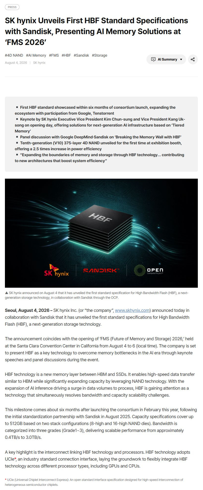
SK hynix Newsroom announcement of the first HBF standard specification at FMS 2026 (up to 512GB per stack, three bandwidth grades, UCIe)
The schedule moved a bit differently. At the same investor day, Sandisk reportedly said it had finished the tape-out (the stage where design is done and handed over for production) of its first HBF die and that customer samples would come next year [6]. A year earlier the target was first samples in the second half of 2026, and this time the wording was customer samples in 2027, so it isn’t clear whether the two refer to the same samples. Still, going by when customers get them in hand, it has become 2027. The sentence that sets the clock even longer comes, if anything, from SK hynix. The newsroom post announcing the consortium launch in February wrote that the industry expects demand for composite memory solutions including HBF to take off around 2030 [2]. At AI Infra Summit in mid-September, SK hynix introduced HBF as a next-generation NAND solution that applies TSV (through-silicon via, a vertical electrode cut through the silicon) like HBM, but it gave no specs or schedule [7].
To square this ledger, I put the MOU press release from a year ago next to the August spec release and looked for the schedule sentence, and the August release had no schedule sentence at all.
There are no named customers yet. Google and Meta are members helping write the spec, and neither has been announced as a buying customer. In late August, NAND Research noted that NVIDIA, AMD, Intel, Broadcom, Marvell, Micron, Samsung, Qualcomm and Western Digital had not joined the consortium, and that the standard is therefore not currently supported by merchant GPU vendors [8].
Records on the other side piled up too. At Hot Chips in August, OXMIQ Labs showed a calculation running the Kimi-K2 model on a 72-GPU rack: at the same cost and power, using only HBF instead of HBM raises capacity by a whopping 14 times, to nearly 300TB, but cuts the rack’s total bandwidth by a little over 40 percent compared with HBM only [9][10]. It also attached conditions, that there is no software support yet and that reads and writes have to happen in large units, and the conclusion was reportedly to put HBM in the rack and HBF in the box [9]. OXMIQ founder Raja Koduri is listed on Sandisk’s HBF technical advisory board in its investor day materials [5]. So this takeaway is closer to a usage map drawn inside the same camp than to outside criticism. NAND’s write endurance keeps coming up as well. One analysis says the KV cache (memory that holds the conversation context), which has to be written anew for every token generated, is more than NAND’s write endurance can handle, so HBF belongs with model weights [11]; there is also an opposing view that the KV cache is mostly reads [12], so where HBF fits best is not settled yet.
That was a long stretch, but if I shrink the ledger to one line, the spec and the consortium came faster than expected, while customers and schedules are coming about a year late. The roundtable answers pointed the same way as this ledger. What I gained on site beyond that was that the temperature was a notch lower than the public record alone would suggest.
Up to here is where the public record and the on-site answers overlap. But at the end of the same answer, the speaker added one more technical reason, and that reason wasn’t a problem for HBF alone. In the paid section I go on to why that reason is a problem of land on the SoC edge, and why a question from the subscriber chat, “What do you think of Micron’s new product?”, is exactly about that land. The on-site answer on microLED optical links, another subscriber’s question asking me to watch Wuhan’s JFS, and the check against my January and August articles come after that.
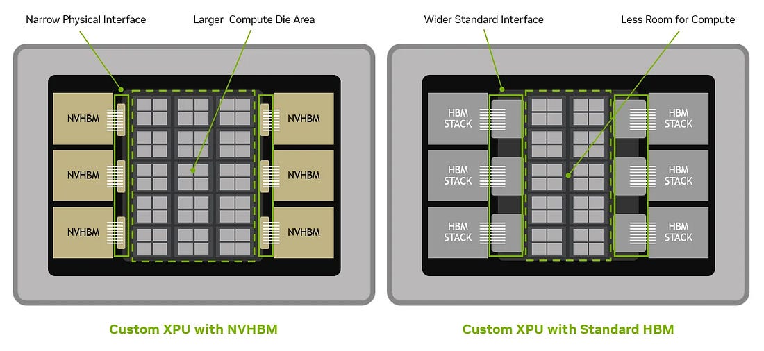
NVIDIA’s NVHBM comparison. NVHBM on the left, standard HBM on the right; with NVHBM the physical interface on the XPU die narrows and the compute die area grows
If you’d like to support my independent research and creative journey, please consider a “pledge.” Your support keeps the photons moving.
 Subscribed
Share this with anyone who needs to see the world through a different wavelength.
Share
3. The Land on the SoC Edge
Here is the reason the speaker added. To put HBF in the same package as HBM, a PHY for HBF has to go on the SoC side, and that, the speaker said, makes no sense from the SoC’s point of view. The PHY is already eating an enormous amount of area now that it has widened to 2K. It’s the same even if you go 3D, the speaker said. For one processor to have both a PHY for the DRAM stacked on top and a PHY for the chip placed beside it, there won’t be any land left, and then things would have to move toward splitting the SoC into chiplets to divide up functions, the explanation went. At the end, the speaker added that it remains to be seen.
A PHY is the physical layer circuit laid along the edge of a chip that actually sends and receives the signals. 2K refers to the HBM4 interface width. Under the JEDEC standard, each HBM4 stack moves data over a 2,048-bit interface, and the number of independent channels doubled from HBM3 to 32 [13]. As the width grew, so did the circuit on the processor die’s edge that receives one HBM stack.
In Beside, Above, or Beyond: The AI Memory Capacity Race and Where Optics Fits on August 16, I called the wall facing the option of placing HBF next to the processor the beachfront. The package edge is already mostly taken by HBM, so if HBF gets one spot, one HBM stack drops out; that was the arithmetic. The roundtable answer looks at the same wall from the processor die’s side. A cramped package floor is a problem, but before that, there isn’t even enough room on the processor die’s edge to put the PHY.

The land on the XPU die edge. With standard HBM4E the memory controller and PHY sit on the XPU die; with NVHBM they sit in the HBM base die. Concept diagram with the candidates for the freed edge (compute, UCIe PHY for HBF, optical I/O)
In the paid subscriber chat, one reader asked what I think of Micron’s new product. The Micron new product talked about most in the first week of October was NVHBM. In its fiscal fourth-quarter earnings materials on September 30, Micron said it is working with NVIDIA on NVHBM, the industry’s first custom HBM4E implementation, and that it will be adopted in next-generation GPUs and NVLink Fusion platforms [14]. On the call, Micron said it co-designed HBM4E with NVIDIA and that the base die (the logic chip at the very bottom of the HBM) is made on a foundry process instead of in-house as with HBM4 [15]. TheElec reported that Micron has handed the HBM4E base die to TSMC, that it is believed to be on a 3-nanometer-class process, and that NVHBM uses the same approach [16].
NVHBM itself was announced first by NVIDIA on August 26. The structure takes the memory controller NVIDIA designed out of the XPU (a term grouping GPUs and custom accelerators) die and moves it into the HBM base die. NVIDIA said that compared with standard HBM4E, memory bandwidth rises by up to 30 percent, HBM power falls by 15 percent, and up to 25 percent more XPU compute die area becomes usable [17]. The developer blog on the same day explained that a custom PHY goes in as well, and wrote that the area of the PHY and its supporting circuitry shrinks by up to a whopping 67 percent versus the JEDEC HBM4E standard [18]. The developer blog put the area freed for compute at 25 percent in one passage and 30 percent in another, so here I use the same 25 percent as the corporate blog. The first partner is Amazon’s Annapurna Labs, and NVIDIA said only that several memory companies will supply it, without naming them [17]. Micron, in effect, put its own name down in its earnings release.
So NVIDIA and Micron have come out with a product that moves off the processor die the very circuit the speaker called enormous in area even with the HBM PHY alone. The direction itself isn’t new. SK hynix also moved its base die to a TSMC logic process starting with HBM4 [19], and at the roundtable, on top of the voltage reason introduced in Part 1, the speaker cited being able to bring in logic IP and fit features customers want into the leftover area. NVHBM goes one step further from there and pushes even the processor-side circuitry down into the base die.
So who takes the land freed up this way? My view is that compute takes it first. NVIDIA itself counted that land as compute die area in its announcement. From an accelerator company’s point of view, the first thing you want to do when the die edge frees up is to put in more compute units and cache. For HBF to come into that land, a UCIe PHY has to be placed separately on the processor side per the spec, and as the speaker said, that is a structure where room appears only after the SoC is split into chiplets and the memory connection function is pulled out into a separate die. So NVHBM reads less like a product that moves HBF’s turn forward and more like one that relieves the pressure in the fight over HBM spots.
Even with the land freed, I think HBF’s turn is still a long way off.
There is one caveat to this arithmetic. Whether the die edge, that is, the beachfront, frees up by as much as the PHY area shrinks depends on the chip layout. Even if the controller moves down into the base die, the connection between the XPU and the base die remains. So I treat only the area and power numbers NVIDIA disclosed as fact, and note that how much the beachfront widens will be known only when real chips come out. I couldn’t find a way to narrow this down further with public material. When you look at CPO packages, how many optical engines you can attach next to the chip ends up being decided by the length of the chip edge. The memory side is fighting the same fight.
Adding one more piece of Micron’s situation answers the question. At least going by public material, Micron is not filling the gap between HBM and SSD with HBF. In the same earnings materials, Micron said AI context memory storage used for KV cache offload is expanding the market for SSDs, and there is not a single line about HBF or optics in the whole document [14]. As noted earlier, Micron’s name isn’t on the HBF consortium list either [8]. To answer the subscriber’s question in one line: Micron’s new product is less an answer on the HBF side than an answer to the problem of HBM eating too much of the processor’s land, and my view is that the land it frees will be used by compute for the time being.
4. Where Optics Comes In
At the same roundtable, an attendee who said they had studied optics asked one more question. The attendee had read the CPO (Co-Packaged Optics, putting optical transceivers in the same package as the processor) review paper published in Nature Electronics in August with an SK hynix researcher as a corresponding author [20], expected it to be about laser-based CPO, and found microLED in it instead; since SK hynix had also invested in Avicena, the question was whether it is working with the microLED side.
The answer went like this. That paper wasn’t the packaging organization’s work, and the memory system side is studying applications that use microLED, the speaker said. The explanation continued that, looking at memory itself, it isn’t clear CPO is needed that much, because optics comes in from the board side. Still, as you do packaging, a situation will come where you can’t afford not to know CPO or anything else, so the team is watching, and seems to be doing something like a PoC project to gauge how effective it might be, the speaker said. The last sentence leaned toward it being hard to say they are doing it seriously yet.
This answer has to be read narrowly. The respondent belongs to the packaging organization and drew a line up front that microLED is another organization’s work. The “it seems” attached here and there throughout the answer also had the tone of relaying another organization’s work secondhand. So what I can say goes as far as the temperature seen from the packaging organization being lukewarm. Neither that the whole company has shelved this technology nor that a big program is running can be drawn from this answer alone.
The public record hasn’t moved much since August. In its August 20 newsroom post, SK hynix listed research on microLED-based massively parallel optical interconnect as future work [20], and as far as I could find, there has been no further primary announcement on optics since mid-September. Ahead of ECOC, on September 17, Avicena released a 1Tbps evaluation kit that can be plugged in and unplugged with a connector. It runs up to 335 microLED channels at up to 3Gbps per channel, and it listed XPU-to-memory links and memory disaggregation as target links [21]. It said it is in discussions with memory manufacturers but named none. There was also a report that Korean venture capital firm Intervest bought new Avicena shares in September [22].

Top of Avicena’s September 17, 2026 press release. The connectorized LightBundle eKit and its list of target links.
I agree with this answer only halfway. For now, it’s right. Looking at a single memory die, the reason to pull optics all the way into the package is weak, and optics gets used first at board and rack distances. That is the placement I called “beyond” in the August article. But as memory pooling, where several XPUs share memory, grows, I think the story changes. Once the path to memory starts crossing the rack, a moment comes when electrical has to be converted to optical at the package boundary where that path begins, and among the uses Avicena listed in its release, XPU-to-memory links and memory disaggregation are exactly that spot. So the packaging organization’s lukewarmness is an answer that comes from today’s distances, and I don’t think it should be read as far as meaning a memory company doesn’t need to know this technology. The speaker personally said a situation would come where they can’t afford not to know it, after all.
Among the three memory makers, the one reported to plan to bring optics all the way next to HBM is Samsung. The report says it will have in-house PIC (photonic integrated circuit) wafer testing in place by the end of 2026, launch a silicon photonics foundry service in 2027, and in the longer run integrate optical engines with logic chips and HBM [23]. It’s at the report level, but the direction is quite different from the temperature I heard from SK hynix’s packaging organization this time.
Another subscriber left a comment on the October 1 silicon photonics foundry article suggesting I keep an eye on Chinese fabs such as Wuhan’s JFS. JFS is the Jiufengshan Laboratory (九峰山实验室) that Hubei Province set up in 2021, and it runs compound semiconductor and silicon photonics pilot lines. According to a 2024 local report carried on the Wuhan city government site, it said it had produced the world’s first optoelectronic integrated wafer combining 8-inch silicon photonics and thin-film lithium niobate [24]. What touches this topic is a microLED joint venture JFS set up with two companies in January this year. The stated business scope is to build on automotive lighting and expand into micro displays and optical interconnect [25]. At CIOE in Shenzhen in September, several Chinese companies brought microLED optical link parts for data centers, and the market research firm TrendForce said microLED-based CPO transceiver modules could enter volume production as early as the second half of 2028 [26]. The picture that drew the microLED optical link supply chain as just a few US startups probably needs fixing now. The technology leakage concern in the comment isn’t something I can verify from public material, so I didn’t carry it over, and I found no record in the US Federal Register of JFS by name being added to an export control list. I plan to cover JFS as a foundry separately in a follow-up to the October 1 article.
5. Checking the January and August Articles

The HBF ledger after eight months. For each item the January article staked out (first samples, standard, customers, optical link, stacking tools): what January said, the public record now, and what was heard at the roundtable. “Named buyers: 0” highlighted
The sentence I put the most weight on in the January 26 article was that HBF was likely to speed up the expansion of the optical interconnect ecosystem. Looking at it now, that link ran ahead. The spec came out as UCIe, an electrical connection inside the package, and to date there has not been a single primary announcement of attaching HBF over optics. The answer from the memory company’s packaging organization also leaned toward asking whether memory alone needs CPO that much. The schedule ran ahead too. The January article carried over SK hynix’s second-half 2026 sampling as is, but the point at which customers get samples in hand is, as of now, 2027. The sentence that HBF would become an essential tier also lacks grounds for a judgment now, with no named customers and even SK hynix’s newsroom putting the demand ramp around 2030, and on stacking equipment demand there is nothing to check yet because the bonding method hasn’t been disclosed. I admit I read the targets the companies stated one step ahead of where they were.
In the August 16 article, I wrote of this January call that the direction was more or less right. Of what I called the direction then, the part about HBF becoming a standard went on as is, while the part about HBF bringing optics along still has no primary evidence, and I separate the two here. The same article attributed Sandisk’s schedule of second-half samples and early-2027 devices to the August spec release, but that schedule came from the August 2025 MOU announcement [1]. I correct that source attribution here as well.
The main argument of the August article stands. The picture was that HBF is a tier whose performance doesn’t suffer much even if it leaves the processor’s side, and that once capacity outgrows the package, the added share piles up on the far side of an optical link. The evidence that appeared over the two months all points toward this picture. At the roundtable I heard that there is no land on the processor side for an HBF PHY and that optics comes in from the board side, and at Hot Chips a calculation came out for putting HBF on the box side [9]. That said, no company has yet said it will release HBF equipment connected over optics. I keep the picture, but I note that the evidence is still circumstantial.
I also checked the bar I set in One Interconnect Company, All Three Memory Makers on the Cap Table: Fifteen Months of SK hynix’s CPO Track on August 20. I wrote that the most valuable marker was whether Avicena would name a memory customer in its next announcement, and the September 17 release listed memory connections as a use yet left out any customer name [21]. It hasn’t been met yet. I’ll keep watching whether SK hynix’s name shows up more in CPO-related primary sources through the first half of 2027, but going by the temperature at the roundtable, that bar seems unlikely to be met for a while. The Credo microLED cable demo, on which I deferred judgment in The Dispersion Problem in microLED Optical Interconnects: Credo’s 30 Meters, MOSAIC’s Data, and the Hyperlume Patent on September 16, is scheduled for OCP next week [27].
6. Closing
HBF and microLED are both cards the memory side played first, yet on the packaging side the temperature was lukewarm for both. Both are coming more slowly than I wrote eight months ago, and what blocks them is the land on the SoC edge more than the technology. NVHBM, which Micron came out with, is the first case of freeing that land, but compute will use the freed land first for the time being. So my view is that the day HBF sits next to the processor comes after the SoC is split into chiplets, and that before then, HBF on the box and board side, and the optical links running to it, settle in first.
That said, it’s possible I’m reading this picture wrong. If Sandisk names an accelerator customer that will carry HBF at its October 29 earnings, or if NVIDIA or another accelerator company says it will put an HBF connection into the next generation of custom base dies, then HBF next to the processor is coming sooner than I think. In that case I’ll have to revise this conclusion. Conversely, if the customer samples promised for next year slip another year, HBF has to be seen as late on the box side too, and the optical increment moves back with it. As for microLED, if a measured optical interface paper for memory comes out under SK hynix’s name or Avicena names a memory customer, the lukewarm temperature I heard this time could change quickly.
Dates to check against:
- October 12-15: OCP Global Summit. Credo’s microLED cable demo [27], Avicena attending. The event preview published in early October lists no HBF session [28]
- October 14-16: SEDEX (COEX). Samsung and SK hynix exhibiting
- Late October (date not announced): SK hynix third-quarter earnings. Whether an HBF schedule or anything on optics comes up for the first time
- October 29: Sandisk fiscal first-quarter earnings [29]. HBF customer sample timing and customer names
- November (expected, not announced): SK AI Summit. The session flagged in the August 20 article
- Early December (expected): Marvell earnings. First revenue timing for Photonic Fabric
- December (expected): Micron fiscal first-quarter earnings. NVHBM timing and whether HBF comes up
- 2027: HBF customer samples, the first accelerator with NVHBM
If you pick just one, watch Sandisk’s earnings on October 29. That’s the day this article’s conclusion could be shaken first.
The forum series ends here. I plan to write separately about the margin and long-term contract talk I heard at the roundtable after all the third-quarter results are out in late October. The middle section of this piece came from two questions in the subscriber chat. Thank you to the two readers who asked.
7. References
1] Sandisk (Business Wire): Sandisk to Collaborate with SK hynix to Drive Standardization of High Bandwidth Flash Memory Technology, 2025-08-06
2] SK hynix Newsroom: SK hynix and Sandisk Begin Global Standardization of Next-Generation Memory ‘HBF’, 2026-02-26
3] SK hynix Newsroom: SK hynix Unveils First HBF Standard Specifications with Sandisk, Presenting AI Memory Solutions at ‘FMS 2026’, 2026-08-04
4] StorageNewsletter: FMS 2026: Sandisk and SK hynix Advance Global Standardization of High Bandwidth Flash with Release of First OCP Technical Specification (full Sandisk release), 2026-08-05
5] Sandisk IR: 2026 Sandisk Investor Day (presentation, HBF Consortium Milestones slide), 2026-08-13
6] TIKR: What SanDisk Stock’s 14% Investor Day Jump Means for a $93.9 Billion Backlog, 2026-08-13 (secondary source)
7] SK hynix Newsroom: SK hynix Presents ‘New Spectrum’ for AI Infrastructure at ‘AI Infra Summit 2026’, 2026-09-17
8] NAND Research: High Bandwidth Flash: Bridging the Gap Between Expensive HBM & Flash Memory, 2026-08-23
9] Tom’s Hardware: Hot Chips 2026: High Bandwidth Flash promises massive bandwidth and capacity, but its usability is extremely limited, 2026-08-26 (secondary source, members only)
10] ServeTheHome: Oxmiq Labs HBF in AI Compute at Hot Chips 2026, 2026-08-27
11] Chipstrat: High Bandwidth Flash: The Full Report, 2026-07-07 (secondary source, free section)
12] HPCwire: What Is High Bandwidth Flash (HBF) and Can It Overcome the AI Memory Wall?, 2026-08-04
13] JEDEC(Business Wire): JEDEC and Industry Leaders Collaborate to Release JESD270-4 HBM4 Standard, 2025-04-16
14] Micron: Fiscal Q4 2026 Earnings Call Prepared Remarks, 2026-09-30
15] The Motley Fool: Micron (MU) Q4 2026 Earnings Call Transcript, 2026-10-01 (secondary source)
16] TheElec: Micron Says NVHBM to Improve Profitability Even With Outsourced Base Die, 2026-10-02
17] NVIDIA Blog: NVIDIA NVLink Fusion Expands With NVHBM Custom High-Bandwidth Memory, 2026-08-26
18] NVIDIA Technical Blog: NVIDIA NVLink Fusion Brings NVHBM to Next-Generation AI Infrastructure, 2026-08-26
19] SK hynix Newsroom: SK hynix at TSMC 2026 Technology Symposium, 2026-04-23
20] SK hynix Newsroom: SK hynix’s technology roadmap for co-packaged optics features in ‘Nature Electronics,’ as AI competition shifts from chips to systems, 2026-08-20
21] Avicena: Avicena to Demonstrate World’s First Connectorized microLED Optical Interconnect for AI Infrastructure at ECOC 2026, 2026-09-17
22] Dealsite: Intervest invests KRW 13.6 billion in US-based Avicena, an AI optical interconnect company (in Korean), 2026-09-30
23] TrendForce: Samsung Reportedly Eyes In-House Silicon Photonics PIC Testing by End-2026 with TSMC-Qualified Tools (citing TheElec), 2026-09-08
24] Wuhan Municipal Government (reprinting Changjiang Daily): Jiufengshan Laboratory debuts the world’s first 8-inch wafer for advanced optoelectronic integrated chips (in Chinese), 2024-04-11
25] Sina Tech: United Nova Technology, Xingyu and Jiufengshan Laboratory plan CNY 3 billion Micro-LED industrialization project (in Chinese), 2026-01-13
26] TrendForce: Micro LED Optical Interconnects Take Center Stage at CIOE 2026, 2026-09-28
27] The Motley Fool: Credo (CRDO) Q1 2027 Earnings Call Transcript, call 2026-09-01, published 2026-09-08 (secondary source)
28] Converge Digest: OCP Global Summit 2026 Preview: AI Fabrics, Optical MSAs and 800 VDC, 2026-10-04
29] Sandisk: Sandisk to Report First Quarter Fiscal Year 2027 Results on October 29, 2026, 2026-09-29
This article is an independent technical analysis published by PhotonCap, based on an engineering perspective. All content is derived from publicly available information and the author’s on-site notes, and remarks heard at the event are identified as such in the text. It is intended solely for educational and informational purposes. In other words, nothing in this material should be construed as a recommendation to buy, sell, or hold any specific securities. Please note this carefully.
The author may hold positions in the securities mentioned herein and reserves the right to trade such securities at any time without prior notice. Readers should conduct their own thorough review and research before making any investment decisions.
Share